UPD72012 Просмотр технического описания (PDF) - NEC => Renesas Technology
Номер в каталоге
Компоненты Описание
Список матч
UPD72012 Datasheet PDF : 36 Pages
| |||
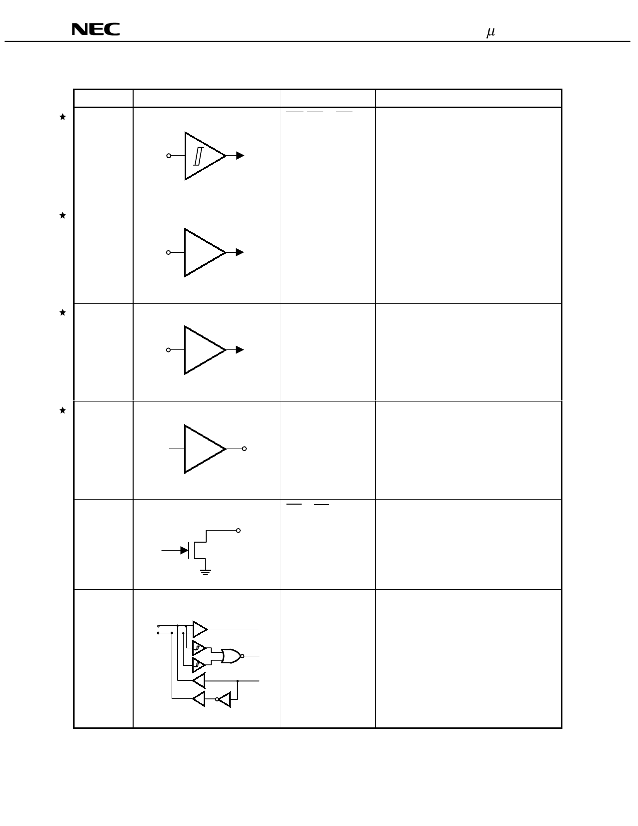
1.3 Equivalent Circuits of Pins
Type
5 V tolerant
input pin
(Schmitt)
Equivalent Circuit
µPD72012
Pins
RST, CS1 to CS5
Function
3.3 V Schmitt input pin with 5 V tolerant.
5 V tolerant
input pin
5 V Schmitt on-chip
CLKSEL, PSSEL,
PVSEL
3.3 V input pin with 5 V tolerant.
5V
5 V tolerant
clock input
pin
5V
5 V tolerant
3.3 V output
pin
Open-drain
output pin
3.3 V, IOL=6 mA
X1, CLK/X2
3.3 V dedicated clock input pin with 5 V
tolerant.
OSL
3.3 V output pin with 5 V tolerant.
Pull-up to 5 V line is possible.
PP1 to PP5
Open-drain structure pin.
USB buffer
IN/OUT(D+)
(D–)
RxDATA
UD0, UD1, D10 to
D50, D11 to D51
RxSE0
TxDATA
USB buffer. The two kinds of receiver are
DATA receiver and SE0 (single end 0) receiver
on the receiving side.
On the sending side, rise and fall times are
managed in the last stage of the buffer in
order to create a difference between low-speed
and full-speed.
Data Sheet S13918EJ3V0DS
11
Share Link: 