RS5C62 Просмотр технического описания (PDF) - RICOH Co.,Ltd.
Номер в каталоге
Компоненты Описание
Список матч
RS5C62 Datasheet PDF : 48 Pages
| |||
RP/RF/RS5C62
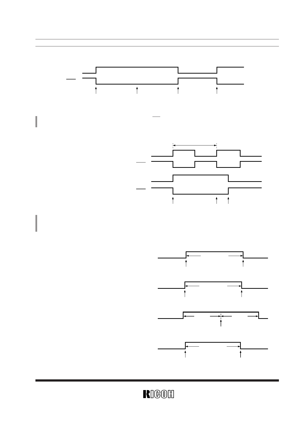
ALFG
INTR
Alarm time match
Alarm time match
Setting the ALFG Alarm time match
bit to “0”
*4) The CTFG bit is set to “1” upon output of a cyclic interrupt from the INTR pin (while it is held low).
(A cyclic interrupt may occur in the pulse mode and the level mode.)
• Pulse mode
(The CT3 bit is set to “0”.)
(The CTFG bit is not intended for write
operation.)
CTFG
INTR
Preset interrupt cycle
• Level mode
(The CT3 bit is set to “1”.)
(The CTFG bit is intended for setting to “0”
only.)
CTFG
INTR
Interrupt
Interrupt Setting the CTFG bit to “0”
*5) When the BSY bit is set to “1”, write operation must not be performed upon the time and calendar counters which are being updated. Normally, read
operation must be performed from the counters upon setting the BSY bit to “0”. Reading from them without checking the BSY bit requires separate
software for preventing reading errors. The BSY bit is set to “1” in the four cases below:
(I) Adjustment by ±30 seconds
(II) Correction by +1
(when there is a 1-second carry in transition of the
WTEN bit from “0” to “1”)
(III) Normal 1-second carry
(IV) Counter resetting (setting of WTRST bit)
(Resetting the 1 to 8Hz dividers)
MAX.122.1µs
Setting the ADJ bit to “1” Completion of adjustment
MAX.122.1µs
Setting the WTEN bit to “1” Completion of correction by +1
91.6µs
30.5µs
Completion of pulse for carry to second digit
MAX.122.1µs
Setting the WTRST bit to “1”
Completion of reset
9
Share Link: 