RS5C62 Просмотр технического описания (PDF) - RICOH Co.,Ltd.
Номер в каталоге
Компоненты Описание
Список матч
RS5C62 Datasheet PDF : 48 Pages
| |||
RP/RF/RS5C62
2. Functions of Registers
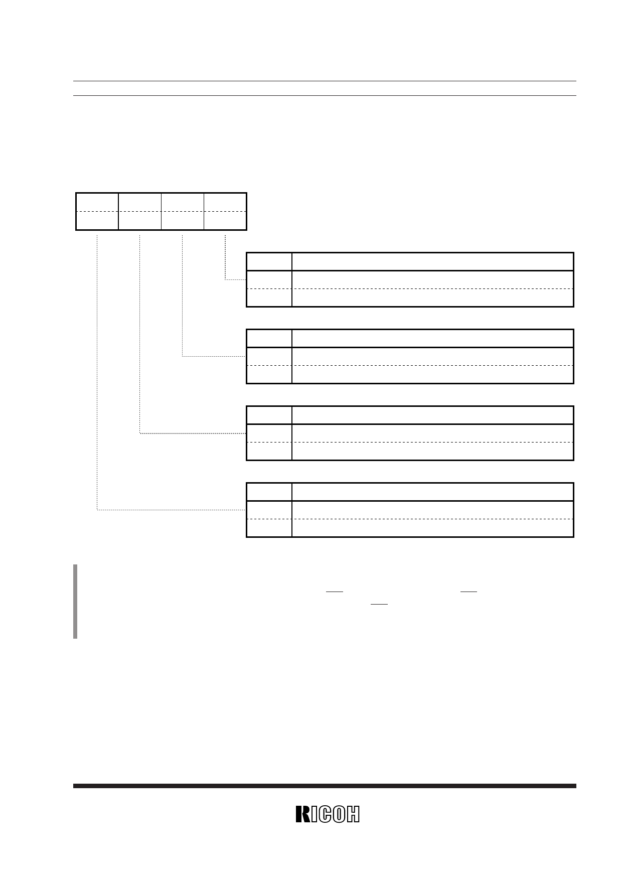
2.1 Control Register 1 (Bank0/1 at “Dh”)
D3
WTEN
0
D2
ALEN
0
D1
TMR
0
D0
BANK
0
(For write operation)
(For read operation) *1
Bank switching bit
BANK
Function
0
Specifies selection of BANK0 in the address table.
1
Specifies selection of BANK1 in the address table.
Timer resetting bit *2
TMR
Function
0
Specifies no change.
1
Specifies resetting of the timer conditional on restart.
Alarm operation setting bit *3
ALEN
Function
0
Disables an alarm interrupt.
1
Enables an alarm interrupt.
Time count operation setting bit *4
WTEN
Function
0
Disables a carry to the 1-second time digit.
1
Enables a carry to the 1-second time digit.
*1) The BANK bit is intended for only write operation and always read as “0”.
*2) The timer frequency can be set by the timer clock selection register.
*3) Setting the ALEN bit to “0” during output of an alarm interrupt from the INTR pin (while it is held low) turns off the INTR pin.
Setting the ALEN bit to “1” in matching between clock time and alarm time drives the INTR pin low within a maximum of 61.1µs.
*4) A 1-second carry with the WTEN bit set to “0” increments the second digit by 1 upon setting of the WTEN bit to “1”. This bit will
automatically be set to “1” upon driving low the CE pin.
7
Share Link: 