IDT723613L30PF Просмотр технического описания (PDF) - Integrated Device Technology
Номер в каталоге
Компоненты Описание
Список матч
IDT723613L30PF
Integrated Device Technology

IDT723613L30PF Datasheet PDF : 29 Pages
| |||
IDT723613 CMOS CLOCKED FIFO WITH BUS MATCHING AND BYTE SWAPPING
64 x 36
COMMERCIAL TEMPERATURE RANGES
FUNCTIONAL DESCRIPTION
FIFO WRITE/READ OPERATION
RESET (RST)
The IDT723613 is reset by taking the reset (RST) input
LOW for at least four port A clock (CLKA) and four port B clock
(CLKB) LOW-to-HIGH transitions. The reset input can switch
asynchronously to the clocks. A device reset initializes the
internal read and write pointers of the FIFO and forces the full-
flag (FF) LOW, the empty flag (EF) LOW, the almost-empty
flag (AE) LOW, and the almost-full flag (AF) HIGH. A reset also
forces the mailbox flags (MBF1, MBF2) HIGH. After a reset,
FF is set HIGH after two LOW-to-HIGH transitions of CLKA.
The device must be reset after power up before data is written
to its memory.
A LOW-to-HIGH transition on the RST input loads the
almost-full and almost-empty offset register (X) with the value
selected by the flag select (FS0, FS1) inputs. The values that
can be loaded into the register are shown in Table 1.
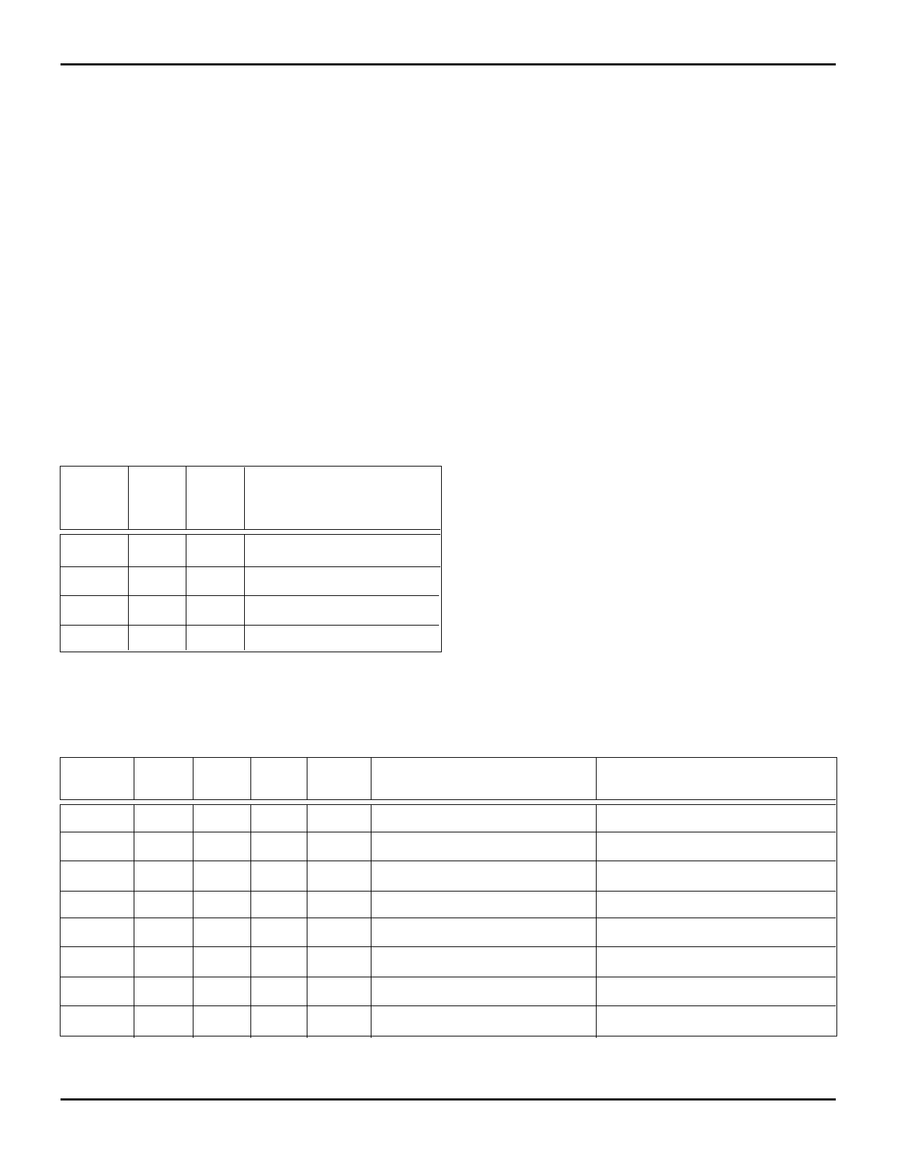
TABLE 1: FLAG PROGRAMMING
ALMOST-FULL AND
FS1
FS0 RST ALMOST-EMPTY FLAG
OFFSET REGISTER (X)
H
H
↑
16
H
L
↑
12
L
H
↑
8
L
L
↑
4
The state of the port A data (A0-A35) outputs is controlled
by the port-A chip select (CSA) and the port-A write/read
select (W/RA). The A0-A35 outputs are in the high-impedance
state when either CSA or W/RA is HIGH. The A0-A35 outputs
are active when both CSA and W/RA are LOW.
Data is loaded into the FIFO from the A0-A35 inputs on
a LOW-to-HIGH transition of CLKA when CSA is LOW, W/RA
is HIGH, ENA is HIGH, MBA is LOW, and FFA is HIGH (see
Table 2).
The state of the port B data (B0-B35) outputs is con-
trolled by the port B chip select (CSB) and the port B write/read
select (W/RB). The B0-B35 outputs are in the high-impedance
state when either CSB or W/RB is HIGH. The B0-B35 outputs
are active when both CSB and W/RB are LOW. Data is read
from the FIFO to the B0-B35 outputs by a LOW-to-HIGH
transition of CLKB when CSB is LOW, W/RB is LOW, ENB is
HIGH, EFB is HIGH, and either SIZ0 or SIZ1 is LOW (see
Table 3).
The setup and hold-time constraints to the port clocks for
the port chip selects (CSA, CSB) and write/read selects (W/
RA, W/RB) are only for enabling write and read operations and
are not related to high-impedance control of the data outputs.
If a port enable is LOW during a clock cycle, the port’s chip
select and write/read select can change states during the
setup and hold time window of the cycle.
SYNCHRONIZED FIFO FLAGS
Each FIFO flag is synchronized to its port clock through
two flip-flop stages. This is done to improve the flags’
reliability by reducing the probability of metastable events on
their outputs when CLKA and CLKB operate asynchronously
to one another. FF and AF are synchronized to CLKA. EF and
AE are synchronized to CLKB. Table 4 shows the relationship
of each port flag to the level of FIFO fill.
TABLE 2: PORT A ENABLE FUNCTION TABLE
CSA W/RA ENA MBA CLKA
H
X
X
L
H
L
L
H
H
L
H
H
L
L
L
L
L
H
L
L
L
L
L
H
X
X
X
X
L
↑
H
↑
L
X
L
↑
H
X
H
↑
A0-A35 OUPTUTS
In high-impedance state
In high-impedance state
In high-impedance state
In high impedence state
Active, mail2 register
Active, mail2 register
Active, mail2 register
Active, mail2 register
PORT FUNCTION
None
None
FIFO write
Mail1 write
None
None
None
Mail2 read (set MBF2 HIGH)
9
Share Link: