CDP1882 Просмотр технического описания (PDF) - Intersil
Номер в каталоге
Компоненты Описание
Список матч
CDP1882 Datasheet PDF : 8 Pages
| |||
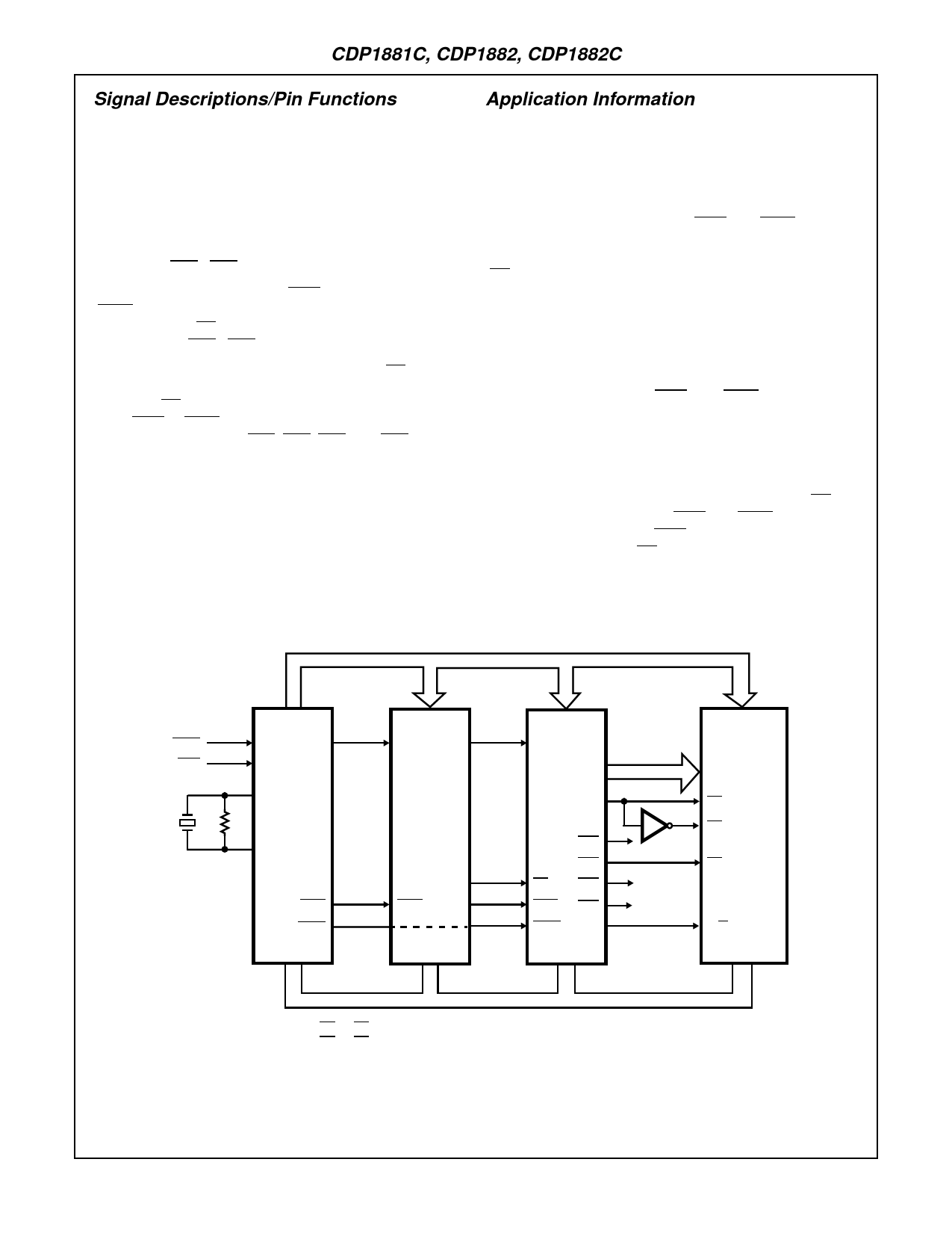
CDP1881C, CDP1882, CDP1882C
Signal Descriptions/Pin Functions
Application Information
CLOCK: Latch-Input Control - a high at the clock input will
allow data to pass through the latch to the output pin. Data is
latched on the high to low transition of the clock input. This
input is connected to TPA in CDP1800-series systems.
MA0 - MA3: Address inputs to the high-byte address
latches.
MA4 - MA5: High byte address inputs decoded to produce
chip selects CS0 - CS3.
MRD, MWR: MEMORY READ (MRD) and MEMORY WRITE
(MWR) signal inputs on the CDP1881C. A low at either
input, when the CE pin is low, will enable the decoder chip
select outputs (CS0 - CS3).
CE: CHIP ENABLE input - a low at the CE input of
CDP1882, CDP1882C will enable the chip select decoder. A
low at the CE input of CDP1881C, coincident with a low at
either MRD or MRW pin, will enable the chip select decoder.
A high on this pin forces CS0, CS1, CS2, and CS3 to a high
(false) state.
A8 - A11: Latched high-byte address outputs.
CS0 - CS3: One of four latched and decoded Chip Select
outputs.
VDD, VSS: Power and ground pins, respectively.
The CDP1881C, CDP1882, CDP1882C can interface
directly with the multiplexed address bus of the CDP1800-
series microprocessor family at maximum clock frequency. A
single CDP1881C or CDP1882 is capable of decoding up to
16K-bytes of memory.
The CDP1881C is provided with MRD and MWR inputs for
controlling bus contention, and is especially useful for inter-
facing with RAMs that do not have an output enable function
(OE). Figure 4 shows the CDP1881C in a minimum system
configuration which includes the CDP1833 ROM (1K x 8)
and two 2K x 8 RAMS. The CDP1881C in this example per-
forms the following functions:
1) Latch and decode high-order address bits for use as chip
selects.
2) Gate chip selects with MRD and MWR to prevent bus
contention with the CPU.
3) Latch high-order address bits A8 to A11.
A system using the CDP1882 is shown in Figure 5. The
CDP1882 performs the memory address latch and decoder
functions. Note that the RAM has an output enable (OE) pin
which eliminates the need for MRD and MWR inputs on the
latch/decoder. Instead, the MRD line is connected directly to
the RAM output enable (OE) pin.
In Figure 6 the CDP1882 is used to decode a 16K-byte ROM
system consisting of four CDM5332s.
WAIT
CLR
TPA
CDP1800
SERIES
CPU
MRD
MWR
ADDRESS BUS
A0 - A7
TPA
CDP1883
1K x 8
ROM
CEO
MRD
MA0 - MA5
CLK
CDP1881C
LATCH/
DECODER
A11
CS0
CS1
CE
CS2
MRD CS3
MWR
A8 - A10
A0 - A7
(2) 2K x 8
RAMS
CEA (NOTE 1)
CEB (NOTE 1)
CS
R/W
DATA BUS
NOTE: CEA = CE RAM NUMBER 1
CEB = CE RAM NUMBER 2
FIGURE 4. MINIMUM 1800-SERIES USING THE CDP1881C
4-6
Share Link: 