PI6C110EV Просмотр технического описания (PDF) - Pericom Semiconductor
Номер в каталоге
Компоненты Описание
Список матч
PI6C110EV Datasheet PDF : 15 Pages
| |||
PI6C110E
Clock Solution for 133 MHz
11223344556677889900112233445566778899001122334455667788990011221122334455667788990011223344556677889900112233445566778899001122112233445566778899001122334455667788990011223344556677889900C112211e22l33e44r5566o77n8899/00P1122e33n4455t66i77u8899m001122I33I44/55I66I7788I9900P11r2211o22c3344e55s66s7788o99r0011s22
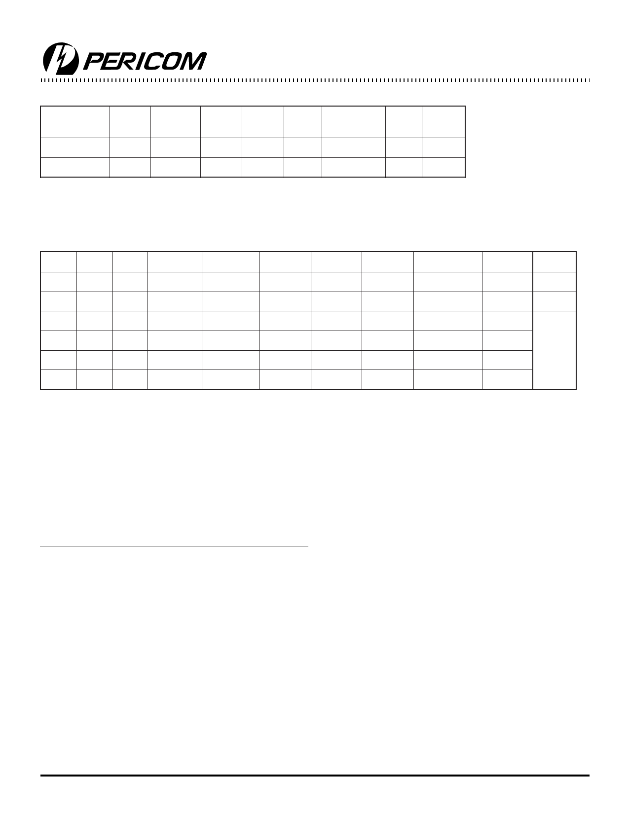
Clock Enable Configuration
PWR_DWN# CPU SDRAM APIC 3V66 PCI
REF,
48 MHZ
Osc VCOs
0
LOW LOW LOW LOW LOW
LOW
OFF OFF
1
ON
ON
ON
ON
ON
ON
ON ON
Notes:
1. LOW means outputs held static LOW.
2. ON means active.
3. PWR_DWN# pulled LOW, impacts all outputs including REF and 48 MHz outputs.
Truth Table
SEL2 SEL1 SEL0 CPU
SDRAM 3V66
PCI 48 MHz
REF
X
0
0
Hi-Z
Hi-Z
Hi-Z
Hi-Z
Hi-Z
Hi-Z
X
0
1 TCLK/2 TCLK/2 TCLK/3 TCLK/6 TCLK/2
TCLK
0
1
0 66 MHz 100 MHz 66 MHz 33 MHz 48 MHz 14.318 MHz
0
1
1 100 MHz 100 MHz 66 MHz 33 MHz 48 MHz 14.318 MHz
1
1
0 133 MHz 133 MHz 66 MHz 33 MHz 48 MHz 14.318 MHz
1
1
1 133 MHz 100 MHz 66 MHz 33 MHz 48 MHz 14.318 MHz
Notes:
1. Required for board level bed of nails testing.
2. Normal mode of operation.
3. TCLK is a test clock over driven on the XTAL_IN input during test mode.
4. Required for DC output impedance verification.
5. Range of reference frequency allowed is min = 14.316 MHz, nominal = 14.31818 MHz, max = 14.32 MHz.
6. Frequency accuracy of 48 MHz is ±167PPM to match 48 MHz default.
APIC
Hi-Z
TCLK/6
33 MHz
33 MHz
33 MHz
33 MHz
Notes
1
3, 4
2, 5, 6
System Clock Design Considerations
PI6C110E supports 4 operational modes. It varies the FSB (Front Side Bus) and SDRAM clock frequencies. FSB selection is 66
MHz, 100 MHz or 133 MHz. SDRAM frequency is either 100 MHz or 133 MHz. The supported modes are:
SEL[2:0] Mode CPU SDRAM 3V66 APIC/PCI
0 1 0 Mode 0 66 100
66
33
0 1 1 Mode 1 100 100
66
33
default
1 1 0 Mode 2 133 133
66
33
1 1 1 Mode 3 133 100
66
33
The clock select pins, SEL[2:0] have the appropriate 100K (±20K) internal pull up and pull down to allow the system defaults to 100 MHz
CPU clock and 100 MHz SDRAM clock without external strapping resistor. SEL2 in pulled down, SEL1 and SEL0 is pulled up to indicate
0 1 1.
The APIC clock is a 33 MHz, the same frequency and phase as the PCI clocks, except it is powered by 2.5V supply. APIC and PCI clocks
are always in phase with the other clocks. In Mode 0, CPU and 3V66 are inverted. In Mode 1 and Mode 3, CPU and SDRAM clocks
are inverted.
System Debug and Timing Margin Analysis
To support system debug and to measure/test margin analysis, the internal PI6C110E oscillator circuits allows the input crystal frequency
to be driven with parallel resonant crystal with frequency range of 10 MHz to 20 MHz in laboratory environment. The alternative is to
put the device in TEST mode, SEL2 = dont care, SEL1 = 1 and SEL0 = 0. Then drive a clock signal to XTAL_IN (pin 3) from
a signal generator and float XTAL_OUT (pin 4).
9
PS8410
08/11/99
Share Link: 