STV0502 Просмотр технического описания (PDF) - STMicroelectronics
Номер в каталоге
Компоненты Описание
Список матч
STV0502 Datasheet PDF : 15 Pages
| |||
STV0502
ELECTRICAL CHARACTERISTICS
Tamb = 25oC, VDD = VCC = 5V, unless otherwise specified (continued)
Symbol
Parameter
Test Conditions
8 BITS ADC & OB CLAMP
OB_rise OB High Time Constant
OB_decay OB Low Time Constant
Pin 38, OB 0 to 1
Pin 38, OB 1 to 0
BLK_RAN Black Level Adjust Range
Pins 8 to 15, OB high,
Serial bus from H00 to H1F
BLK_res
BLK_LEV
ADC_DN
fCLK
tPCLK
Black Level Adjust Resolution
Black Level Adjust
ADC Input Dynamic Range (output
from 0 to 255)
ADC Clock Frequency
Output Pipeline Delay (3)
Pins 8 to 15, per serial bus LSB step
Pins 8 to 15
Bus = H00
Bus = H1F
Pin 38 test signal above black
clamping level (VBOT)
Pin 24
From a sampling to data out
tDADC
RLADD
VTOP
VBOT
ADC_lin
Clock to Data Out (4)
Ladder Resistance
Top Reference Voltage
Bottom Reference Voltage
ADC Linearity
CLK positive edge, CLOAD = 20pF
Between Pins 36 and 37
Pin 36
Pin 37
Data out, input signal between
[VBOT + 25mV ; VTOP - 25mV]
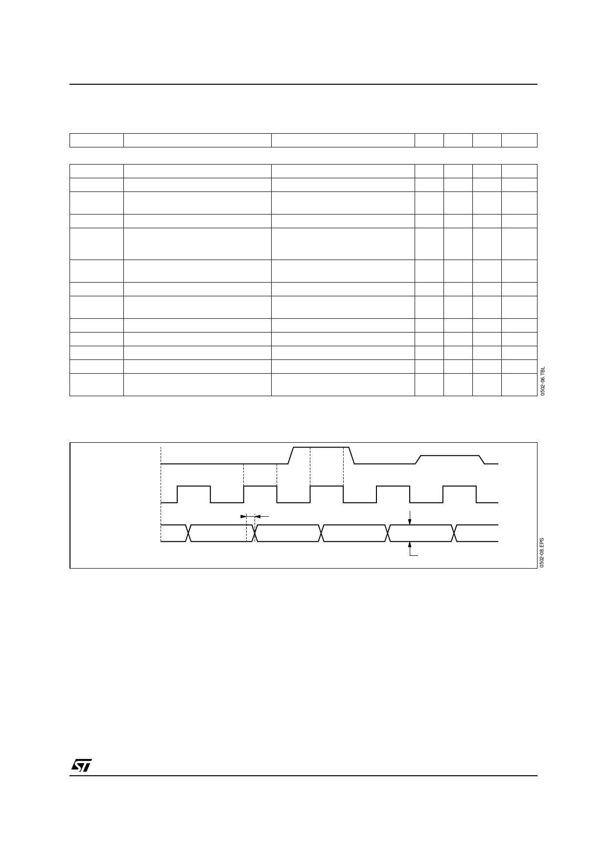
Notes : 3. The signal is being sampled as long as ADC_CLK is high.
4. See Figure 6 for data reading timing constraint.
Min.
4
29
1.4
3
3.2
1.71
Typ.
31
1
0
31
1.55
12
17
330
3.35
1.8
Max.
-2
2
33
1.7
3
3.5
1.89
1
Unit
mV/µs
mV/ms
LSBs
LSBs
LSBs
LSBs
VPP
MHz
CLK
cycles
ns
Ω
V
V
%
Figure 6
ADC_IN
ADC_CLOCK
Sampling
Period
Pixel N
Pixel N+1
DATA_OUT
Pixel N-4
tDADC
Pixel N-3
Pixel N-2
Pixel N-1
Pixel N
Data available
on falling edge of clock
Due to tDADC, and to make sure the data are read when they are stable, please read the data on the falling
edge of the ADC clock.
9/15
Share Link: 