STV0502 Просмотр технического описания (PDF) - STMicroelectronics
Номер в каталоге
Компоненты Описание
Список матч
STV0502 Datasheet PDF : 15 Pages
| |||
STV0502
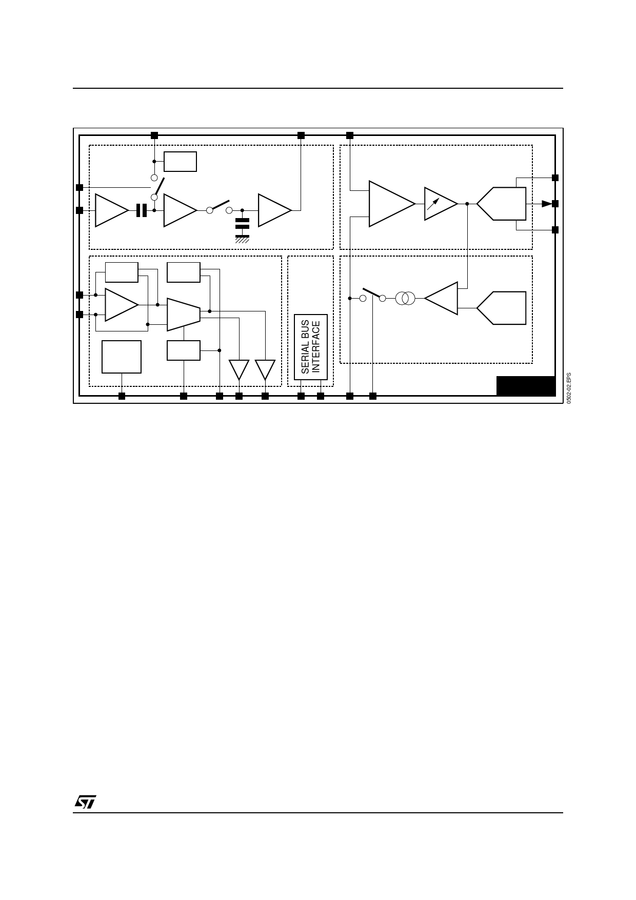
BLOCK DIAGRAM
G=1
VREF
G=1
CORRELATED
DOUBLE
SAMPLING
G=1
BIAS
G=1
BIAS
AUDIO
INTERFACE
VIDEO GAIN AMPLIFIER &
A/D CONVERTER INTERFACE
6dB/18dB
Range
0-18dB
A/D CONV
COMP
D/A CONV
VREG
PSRR
AGC
BLACK LEVEL
ADJUST & CLAMP
STV0502
FUNCTIONAL DESCRIPTION
1 - Video Section
A CCD signal is provided to the STV0502, via a
coupling capacitor, as well as the pulses FS/FCDS.
The CDS (Correlated Double Sampling) is perform-
ing a clamp of the CCD signal during the FCDS
pulse. The signal obtained is then sampled during
the FS pulse, and held the rest of the period. The
resulting signal is then the difference between the
useful pixel level, and the pixel level corresponding
to no charge which can vary from one pixel to
another. Therefore, the parasitic level offset from
one pixel to another is removed.
This signal is DC coupled to the ACG, amplified by
a variable gain amplifier, bus controlled
(0.07dB step), which gain is in the range +6dB to
+23.7dB (17.7dB range). Typically, the amplifier is
controlled in order to keep the signal at an optimum
level (AGC) to be digitized. An extra 12dB can be
added up via a bit of the serial interface. In this case
the gain range becomes +18dB up to + 36dB.
At this point, the signal is clamped to a Black level
during the OB pulse. The black level is 5 bits bus
controlled, and its range corresponds to
[0 LSB ; 31 LSB] of the ADC. The black level is
made with a 5 bits DC frequency DAC, using the
same VBOTTOM and VTOP voltage references than
the ADC for matching purposes. The clamp is made
out of a OB pulse sampled comparator between the
DAC output voltage (Black) and the ADC input
signal. The comparator has a symetrical current
output charging a capacitor. The obtained voltage
is buffered and used as a feedback to the AGC
input stage. This clamp makes sure that ADCin is
matched to the DAC black setting during the OB
pulse, disregarding any offset in the AGC path.
Then the signal is digitized by a fast ADC, clocked
at the pixel rate. The output of the chip is then an
8-bit pixel DATA, ready for digital post-processing.
2 - Audio Section
The chip integrates a high gain audio amplifier, in
order to process low signals coming from a speech
microphone, and provide on its output a line level,
differential audio signal, for digital conversion, or
power amplification. Two modes can be selected :
fixed gain mode or AGC mode. In case of AGC
mode, a peak detection of the signal is performed
in order to regulate the output signal on a defined
level of 1.5VPP or 1VPP (non-diff). This regulated
level can be chosen at 1.5VPP or 1VPP thanks to a
pin at respectively ground or supply voltage (a pull-
up resistor to supply is already included on chip),
for compatibility purposes between the 502 and
various back-end chips.
The system includes a Low-Noise fixed amplifier
(26dB), and a bias circuitry at the front.
3/15
Share Link: 