STB19NM65N Просмотр технического описания (PDF) - STMicroelectronics
Номер в каталоге
Компоненты Описание
Список матч
STB19NM65N
N-channel 650 V - 0.25 Ω - 15.5 A - TO-220/FP-D2/I2PAK-TO-247 second generation MDmesh™ Power MOSFET
STMicroelectronics

STB19NM65N Datasheet PDF : 19 Pages
| |||
STB19NM65N-STI19NM65N-STF19NM65N-STP/W19NM65N
2
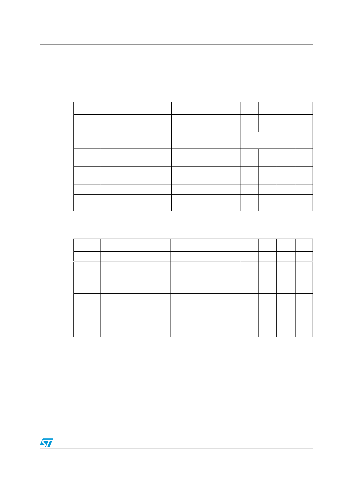
Electrical characteristics
Electrical characteristics
(TCASE=25°C unless otherwise specified)
Table 5. On/off states
Symbol
Parameter
Test conditions
Min. Typ. Max. Unit
Drain-source
V(BR)DSS breakdown voltage
dv/dt (1) Drain source voltage slope
IDSS
IGSS
VGS(th)
RDS(on)
Zero gate voltage
drain current (VGS = 0)
Gate-body leakage
current (VDS = 0)
Gate threshold voltage
Static drain-source on
resistance
ID = 1 mA, VGS = 0
650
VDD= 520 V, ID=15.5 A,
VGS=10 V
VDS = Max rating
VDS = Max rating, @125 °C
VGS = ± 20 V
VDS = VGS, ID = 250 µA
2
VGS = 10 V, ID = 7.75 A
V
30
V/ns
1 µA
100 µA
±100 nA
3
4
V
0.25 0.27 Ω
1. Characteristics value at turn off on inductive load
Table 6. Dynamic
Symbol
Parameter
Test conditions
Min. Typ. Max. Unit
gfs (1)
Ciss
Coss
Crss
Forward transconductance
Input capacitance
Output capacitance
Reverse transfer
capacitance
VDS=15 V, ID =7.75 A
VDS = 50 V, f = 1 MHz,
VGS = 0
15
S
1900
pF
110
pF
10
pF
Coss
(2)
eq.
Equivalent output
capacitance
VGS = 0 ,
VDS = 0 to 520 V
230
pF
Qg Total gate charge
Qgs Gate-source charge
Qgd Gate-drain charge
VDD = 520 V, ID = 15.5 A,
VGS = 10 V,
(see Figure 19)
55
nC
9
nC
30
nC
1. Pulsed: pulse duration = 300µs, duty cycle 1.5%
2. Coss eq. is defined as a constant equivalent capacitance giving the same charging time as Coss when VDS
increases from 0 to 80% VDSS
5/19
Share Link: