UT62L12916 Просмотр технического описания (PDF) - Utron Technology Inc
Номер в каталоге
Компоненты Описание
Список матч
UT62L12916 Datasheet PDF : 12 Pages
| |||
Rev. 1.0
UTRON
UT62L12916/UT62L12916(I)
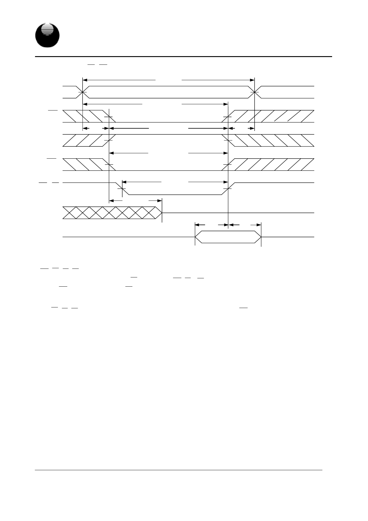
128K X 16 BIT LOW POWER CMOS SRAM
WRITE CYCLE 3 ( LB , UB Controlled) (1,2,5,6)
tWC
Address
tAW
CE
tAS
tCW
tWR
CE2
tWP
WE
LB , UB
Dout
Din
tWHZ
tBW
High-Z
tDW
tDH
Data Valid
Notes :
1. WE , CE , LB , UB must be high or CE2 must be low during all address transitions.
2.A write occurs during the overlap of a low CE , high CE2, low WE , LB or UB =low.
3.During a WE controlled write cycle with OE low, tWP must be greater than tWHZ+tDW to allow the drivers to turn off and data to be
placed on the bus.
4.During this period, I/O pins are in the output state, and input signals must not be applied.
5.If the CE , LB , UB low transition and CE2 high transition occurs simultaneously with or after WE low transition, the outputs remain in a
high impedance state.
6.tOW and tWHZ are specified with CL = 5pF. Transition is measured ±500mV from steady state.
UTRON TECHNOLOGY INC.
1F, No. 11, R&D Rd. II, Science-Based Industrial Park, Hsinchu, Taiwan, R. O. C.
TEL: 886-3-5777882 FAX: 886-3-5777919
8
P80042
Share Link: 