RF2968 Просмотр технического описания (PDF) - RF Micro Devices
Номер в каталоге
Компоненты Описание
Список матч
RF2968 Datasheet PDF : 20 Pages
| |||
Preliminary
RF2968
Pin Function Description
Interface Schematic
29 RESNTR+ See pin 28.
30
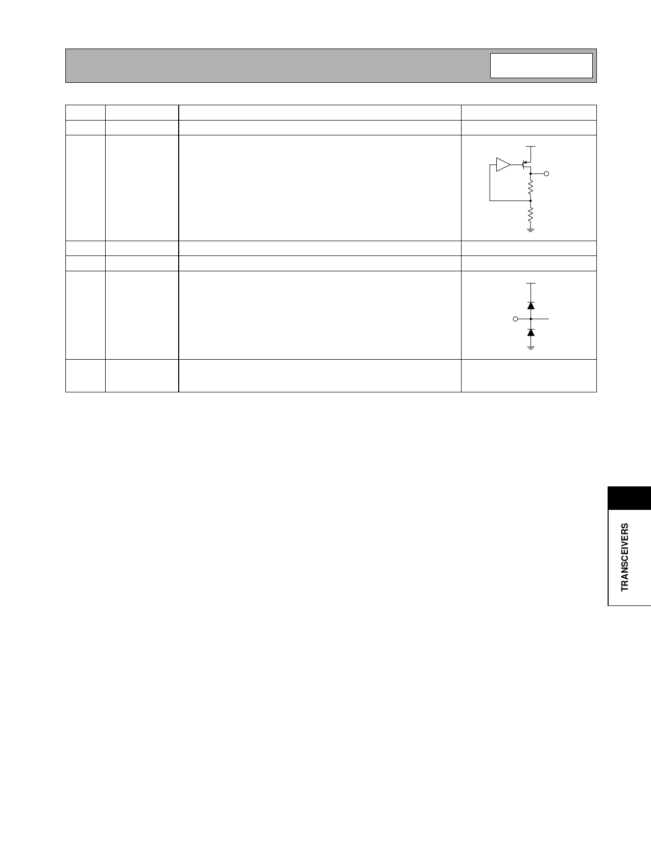
VREG
Voltage Regulator Output (2.2V). A bypass capacitor from this pin to
VCC
ground is required. This voltage is used to bias the VCO through the
tank circuit tied to pins 28 and 29.
VREG
31
IFDGND Ground connection for the digital IF circuits.
32
VCC7
Supply voltage for the digital IF circuits.
ESD
This diode structure is used to provide electrostatic discharge protec-
VCC
tion to 3kV using the Human body model. The following pins are pro-
tected: 6-7, 9-17, 20-27, 30-32.
Die
Flag
GND
Ground connection for all circuits other than those grounded through
dedicated pins. The die flag must be connected to the ground plane
with very low inductance for best performance.
11
Rev A13 010912
11-123
Share Link: 