RF2968 Просмотр технического описания (PDF) - RF Micro Devices
Номер в каталоге
Компоненты Описание
Список матч
RF2968 Datasheet PDF : 20 Pages
| |||
RF2968
Preliminary
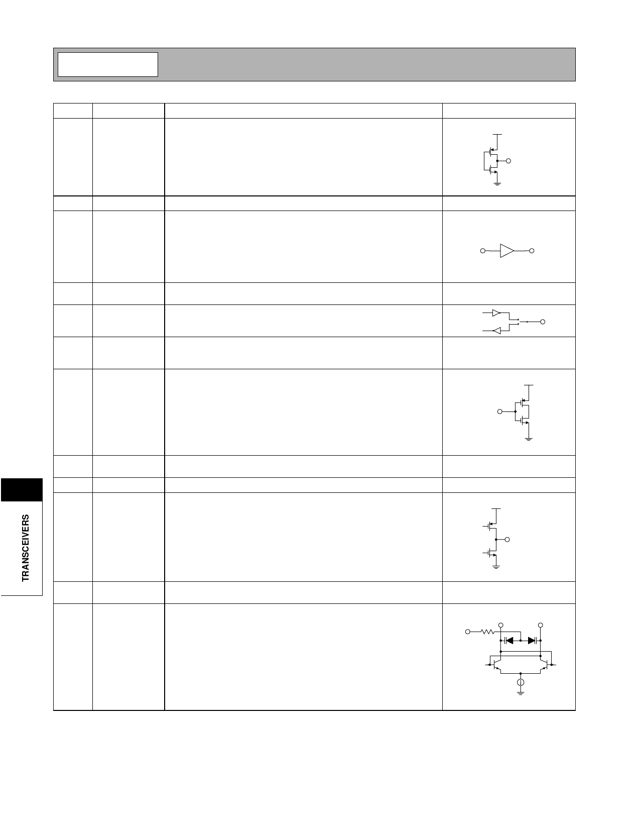
Pin Function Description
Interface Schematic
17
BRCLK Reference clock output. This is a crystal controlled reference clock in
the 10-40MHz range, typically 13MHz.
VCC
BRCLK
18
OSC O Same as pin 19.
See pin 19.
19
OSC I
The OSC pins are used to produce the reference frequency by means
of negative feedback. A crystal and resistor are placed in parallel from
OSC I to OSC O to provide the feedback path and establish the reso-
nant frequency. A shunt capacitor is placed on each OSC pin to provide
OSC I
the proper loading of the crystal. If an external reference is used, it is
connected to OSC I through a DC-blocking capacitor, and OSC O is
connected to OSC I through a 470kΩ resistor.
20
BnDEN Latches data entered into the serial port. Data is clocked into the latch See pin 23.
on the rising edge of BnDEN.
21
BDDATA Serial data port. Read/write data is sent through this pin into / out of the READ DATA
on chip shift register. Read data is transferred on the rising edge of
BDCLK. Write data is transferred on the falling edge of BDCLK.
WRITE DATA
22
BDCLK Serial port input clock.This pin is used to clock data into the serial port. See pin 23.
To minimize the hop frequency programming time, a BDCLK frequency
of 10-20MHz is recommended.
23
BnPWR This pin is part of the chip power control circuit. It is used to power up
the chip from the “off” state.
OSC O
Pin 21
VCC
BnPWR
11
24
PLL GND Ground connection for the RF synthesizer, crystal oscillator, and serial
port.
25
VCC6
Supply voltage for the RF synthesizer, crystal oscillator, and serial port.
26
D0
This is the output of the charge pump for the RF PLL. An RC network
from this pin to ground is used to establish the PLL bandwidth. To mini-
mize synthesizer settling time and phase noise, a dual loop bandwidth
scheme is implemented. During the initial period of frequency acquisi-
tion, a wide loop bandwidth is used. RSHUNT is used to switch to a
narrow loop bandwidth near the end of the frequency acquisition, pro-
viding improved VCO phase noise. The time at which the bandwidth
switches is set by the PLLDel bits.
VCC
D0
27
RSHUNT Switches the loop filter from wide to narrow bandwidth by shunting the
midpoint of two external series resistors to ground.
28
RESNTR- The RESNTR pins are used to supply DC voltage to the VCO as well
as to tune the center frequency of the VCO. Two inductors are required
RESNTR+ RESNTR-
between RESNTR- and RESNTR+ to resonate with the internal capac- D0
itance. Inductance of traces from the RESNTR pins to the inductor
4 kΩ
should be taken into account in the board layout.
11-122
Rev A13 010912
Share Link: 