QT300 Просмотр технического описания (PDF) - Quantum Research Group
Номер в каталоге
Компоненты Описание
Список матч
QT300 Datasheet PDF : 14 Pages
| |||
4.1 1W UART Specifications
The QT300 operates in 1W UART mode with the following
specifications:
Baud rate range
Data length
Stop bit
Parity
Idle state
4,800 to 9,600 bits/sec
2 bytes (16 bits total)
1 (each byte)
None
High
The 1W line must have a pullup resistor on it (i.e. 10K), or
1W communications will not function.
4.2 UART 1W Protocol
The QT300 acquires and transmits only on request. The
sequence is:
1) Host generates pulse on 1W pin; pulse width must
match Baud rate (bit width) of desired return rate. This
actually sets the Baud rate, so it can vary from one
acquire to another. See Section 4.3 and Figure 4-1.
2) The 1W pulse width is measured by the QT300 to
determine the Baud rate.
3) The host floats 1W high.
4) The QT300 acquires the signal to completion.
5) QT300 returns data in the following UART format:
start bit (low)
8 bits, high byte
stop bit (high)
delay (determined by MLS setup)
start bit (low)
8 bits, low byte
stop bit (high)
6) The QT300 floats the 1W line and enters idle mode.
4.3 Trigger pulse description
The part wakes from low power mode when the first negative
edge is detected on the 1W pin (Figure 4-1, bottom). The
negative pulse must be at least 30µs wide.
The host then generates the positive pulse that actually sets
the Baud rate. The QT300 measure this pulse and uses its
length to set the Baud bit (shift out) rate. 30µs (or more) of
logic-low must follow this pulse.
The host must then float the 1W line to allow the QT300 to
start the signal acquisition.
5 Circuit Guidelines
5.1 Sample capacitors
Cs capacitors can be virtually any plastic film or low to
medium-K ceramic capacitor. The normal usable Cs range is
from 1nF ~ 500nF depending on the sensitivity required;
larger values of Cs require higher stability to ensure low drift.
Acceptable capacitor types include NP0 or C0G ceramic,
PPS film, and Y5E and X7R ceramics in that order.
5.2 Power Supply
5.2.1 STABILITY
The QT300 makes use of the power supply as a reference
voltage. The acquired signal will shift slightly with changes in
Vdd; Vdd fluctuations often happen when additional loads
are switched on or off such as LEDs etc.
If the power supply is shared with another electronic system,
care should be taken to assure that the supply is free of
spikes, sags, and surges. It is best practice to use a
regulator just for the QT300 (or one for a set of QT300's).
5.2.2 SUPPLY REQUIREMENTS
Vdd can range from 2 to 5 volts nominal. Current drain will
vary depending on Vdd. During writing of the internal
EEPROM, Vdd must be at least 2.2 volts.
If desired, the supply can be regulated using a conventional
regulator, for example CMOS LDO regulators, or standard
78Lxx-series 3-terminal devices.
For proper operation a 100nF (0.1uF) ceramic bypass
capacitor must be used between Vdd and Vss; the bypass
cap should be placed very close to the Vdd and Vss pins.
5.3 PCB LAYOUT
5.3.1 GROUND PLANES
The use of ground planes around the device is encouraged
for noise reasons, but ground or power should not be
coupled too close to the sense pins in order to reduce Cx
load. Likewise, the traces leading from the sense pins to the
electrode should not be placed directly over a ground plane;
rather, the ground plane should be relieved by at least 3
times the width of the sense traces directly under it, with
periodic thin bridges over the gap to provide ground
continuity.
5.3.2 NOISE SYNCHRONIZATION
External fields can cause interference leading to a noisy and
unstable signal. The most common external fields usually are
from AC mains power.
The /REQ line of the QT300 can be used to synchronize the
acquisition to a repetitive external source of interference
such as the power line frequency in order to dramatically
reduce signal noise.
If line frequency is present near the sensors, this feature
should be used.
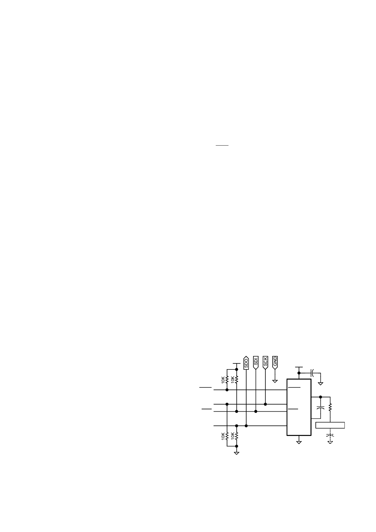
DRDY
SCK
REQ
SDI
Figure 6-1 Clone interface wiring
CLONING SIGNAL
Vdd
Vdd
100nF
QT300 8
Vdd
1 DRDY
SNS1 3
2 SCK
6 REQ
SNS2 5
Rs
Cs
7 SDO
ELECTRODE
Vss
4
Cx
LQ
6
QT300 R1.02/0204
Share Link: 