W83196S-14 Просмотр технического описания (PDF) - Winbond
Номер в каталоге
Компоненты Описание
Список матч
W83196S-14 Datasheet PDF : 15 Pages
| |||
Preliminary W83196S-14
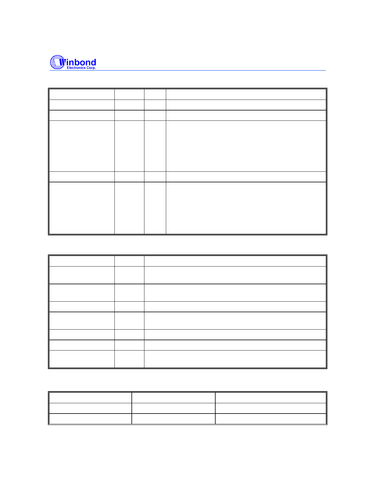
5.4 Fixed Frequency Outputs
SYMBOL
SEL100/66#
IOAPIC
REF2X / SEL48*
24/48MHz
48MHz/Mode*
PIN
I/O
FUNCTION
16
IN CPU clock frequency select pin.
24
O Provides 14.318 fixed frequency.
27
I/O Internal 250kΩ pull-up.
Latched input for SEL48* at initial power up.
SEL48* = 1 , pin14 is 24 MHz
SEL48* = 0 , pin14 is 48 MHz
Reference clock during normal operation.
14
O Frequency is set by the state of pin 27 on power up.
13
I/O Internal 250kΩ pull-up.
48 MHz output for USB during normal operation.
Latched input for Mode* at initial power up. Mode* = 0 ,
then pin10 is PCI_STOP#, and pin11 is CPU_STOP#.
Mode* = 1.(default), pin10 is PCICLK5 and pin11 is
PCLCLK6.
5.5 Power Pins
SYMBOL
VDDCore
VDDP
VDDA
VDDC
VDD4
VDDR
VssC, VssR, Vss4,
VssP
PIN
FUNCTION
20 Power supply for core logic and PLL circuitry. Connect to 3.3V
supply.
9 Power supply for PCICLK_F and PCICLK 1:6. Connect to 3.3V
supply.
25 Power supply for IOAPIC output, Connect to 2.5V supply
23 Power supply for CPUCLK _F and CPUCLK1. Connect to 2.5V
supply.
12 Power supply for 48mhz USB clock . Connect to 3.3V supply.
26 Power supply for 14.318mhz ISA clock . Connect to 3.3V supply.
3, 15, 19, Circuit Ground.
28
6. FREQUENCY SELECTION
SEL100/66#
1
0
CPUCLK_F, CPUCLK1
100 MHz
66.8 MHz
PCI
33.3 MHz
33.3 MHz
-4-
Share Link: 