W83196S-14 Просмотр технического описания (PDF) - Winbond
Номер в каталоге
Компоненты Описание
Список матч
W83196S-14 Datasheet PDF : 15 Pages
| |||
Preliminary W83196S-14
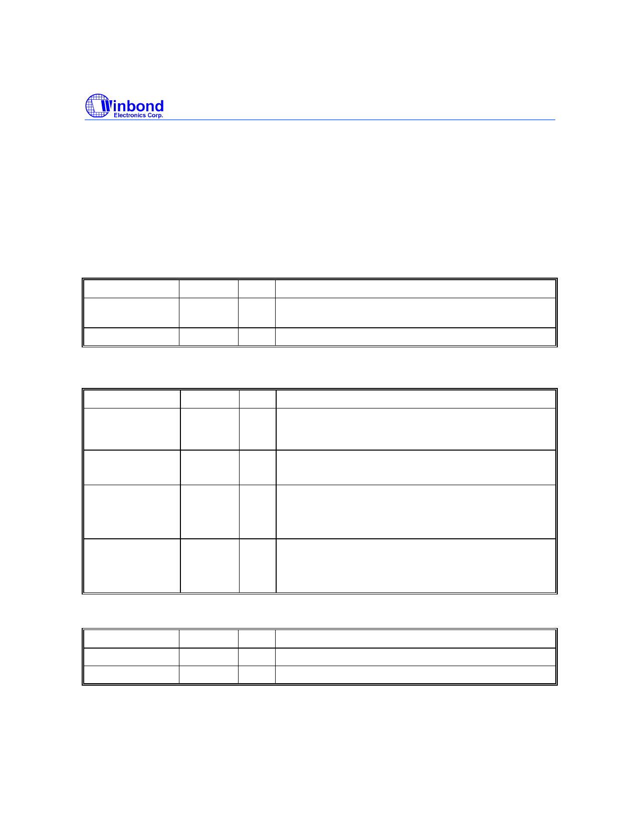
5. PIN DESCRIPTION
IN - Input
OUT - Output
I/O - Bi-directional Pin
# - Low active
* - Internal 250kΩ pull-up
5.1 Crystal I/O
SYMBOL
Xin
Xout
PIN
I/O
FUNCTION
1
IN Crystal input with internal loading capacitors and feedback
resistors.
2
OUT Crystal output at 14.318 MHz nominally.
5.2 CPU, PCI Clock Outputs
SYMBOL
CPUCLK_F
CPUCLK1
PCICLK [ 1:4 ]
PCICLK_F
PCICLK5/
PCI_STOP#
PCICLK6/
CPU_STOP#
PIN
I/O
FUNCTION
22, 21
OUT Low skew (<250 pS) clock outputs for host frequencies
such as CPU, Chipset and Cache. VDDC is the supply
voltage for these outputs.
4, 5, 6, 7, 8 OUT Low skew (<250 pS) PCI clock outputs.
10
I/O If Mode* =1 (default), then this pin is a PCICLK5 buffered
output of the crystal. If Mode* = 0 , then this pin is
PCI_STOP# input used in power management mode for
synchronously stopping the all CPU clocks.
11
I/O If Mode* = 1 (default), then this pin is a PCICLK6 clock
output. If Mode* = 0 , then this pin is CPU_STOP # and
used in power management mode for synchronously
stopping the all PCI clocks.
5.3 I2C Control Interface
SYMBOL
PIN
SDATA*
18
SDCLK*
17
I/O
FUNCTION
I/O Serial data of I2C 2-wire control interface
IN Serial clock of I2C 2-wire control interface
Publication Release Date: March 1999
-3-
Revision A1
Share Link: 