W83178S Просмотр технического описания (PDF) - Winbond
Номер в каталоге
Компоненты Описание
Список матч
W83178S Datasheet PDF : 7 Pages
| |||
Preliminary W83178S
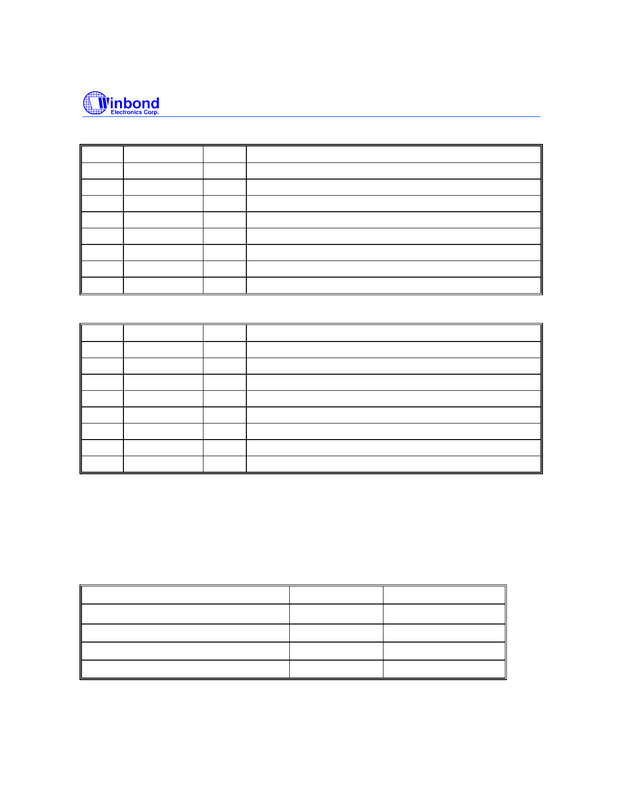
6.2.2 Register 1: (1 = Active, 0 = Inactive)
BIT @POWERUP PIN
DESCRIPTION
7
1
27 SDRAM11 (Active/Inactive)
6
1
28 SDRAM10 (Active/Inactive)
5
1
23 SDRAM9 (Active/Inactive)
4
1
22 SDRAM8 (Active/Inactive)
3
1
-
Reserved
2
1
-
Reserved
1
1
19 SDRAM7 (Active/Inactive)
0
1
18 SDRAM6 (Active/Inactive)
6.2.3 Register 2: (1 = Active, 0 = Inactive)
BIT @POWERUP PIN
DESCRIPTION
7
x
-
Reserved
6
1
12 SDRAM12 (Active/Inactive)
5
x
-
Reserved
4
x
-
Reserved
3
x
-
Reserved
2
x
-
Reserved
1
x
-
Reserved
0
x
-
Reserved
7.0 SPECIFICATIONS
7.1 Absolute Maximum Ratings
Stresses greater than those listed in this table may cause permanent damage to the device.
Precautions should be taken to avoid application of any voltage higher than the maximum rated
voltages to this circuit. Maximum conditions for extended periods may affect reliability. Unused inputs
must always be tied to an appropriate logic voltage level (Ground or VDD).
PARAMETER
SYMBOL
RATING
Voltage on any pin with respect to GND
Storage Temperature
VDD, VIN
TSTG
-0.5V to +7.0V
-65° C to +150° C
Ambient Temperature
TB
-55° C to +125° C
Operating Temperature
TA
0° C to +70° C
Note: Exposure to conditions beyond those listed under Absolute Maximum Ratings may adversely affect the life and reliability of the
device.
-4-
Share Link: 