W83178S Просмотр технического описания (PDF) - Winbond
Номер в каталоге
Компоненты Описание
Список матч
W83178S Datasheet PDF : 7 Pages
| |||
Preliminary W83178S
6. FUNCTIONAL DESCRIPTION
6.1 2-Wire I2C Control Interface
The clock generator is a slave I2C component which can be read back the data stored in the latches
for verification. All proceeding bytes must be sent to change one of the control bytes. The 2-wire
control interface allows each clock output individually enabled or disabled. On power up, the
W83178S initializes with default register settings, and then it’optional to use the 2-wire control
interface.
The SDATA signal only changes when the SDCLK signal is low, and is stable when SDCLK is high
during normal data transfer. There are only two exceptions. One is a high-to-low transition on SDATA
while SDCLK is high used to indicate the beginning of a data transfer cycle. The other is a low-to-
high transition on SDATA while SDCLK is high used to indicate the end of a data transfer cycle. Data
is always sent as complete 8-bit bytes followed by an acknowledge generated.
Byte writing starts with a start condition followed by 7-bit slave address and [1101 0010], command
code checking [0000 0000], and byte count checking. After successful reception of each byte, an
acknowledge (low) on the SDATA wire will be generated by the clock chip. Controller can start to
write to internal I2C registers after the string of data. The sequence order is as follows:
Bytes sequence order for I2C controller:
Clock Address
A(6:0) & R/W
Ack
8 bits dummy
Command code
Ack
8 bits dummy
Byte count
Ack
Byte0,1,2...
until Stop
Set R/W to 1 when read back the data sequence is as follows:
Clock Address
A(6:0) & R/W
Ack
Byte 0
Ack
Byte 1
Ack
Byte2, 3, 4...
until Stop
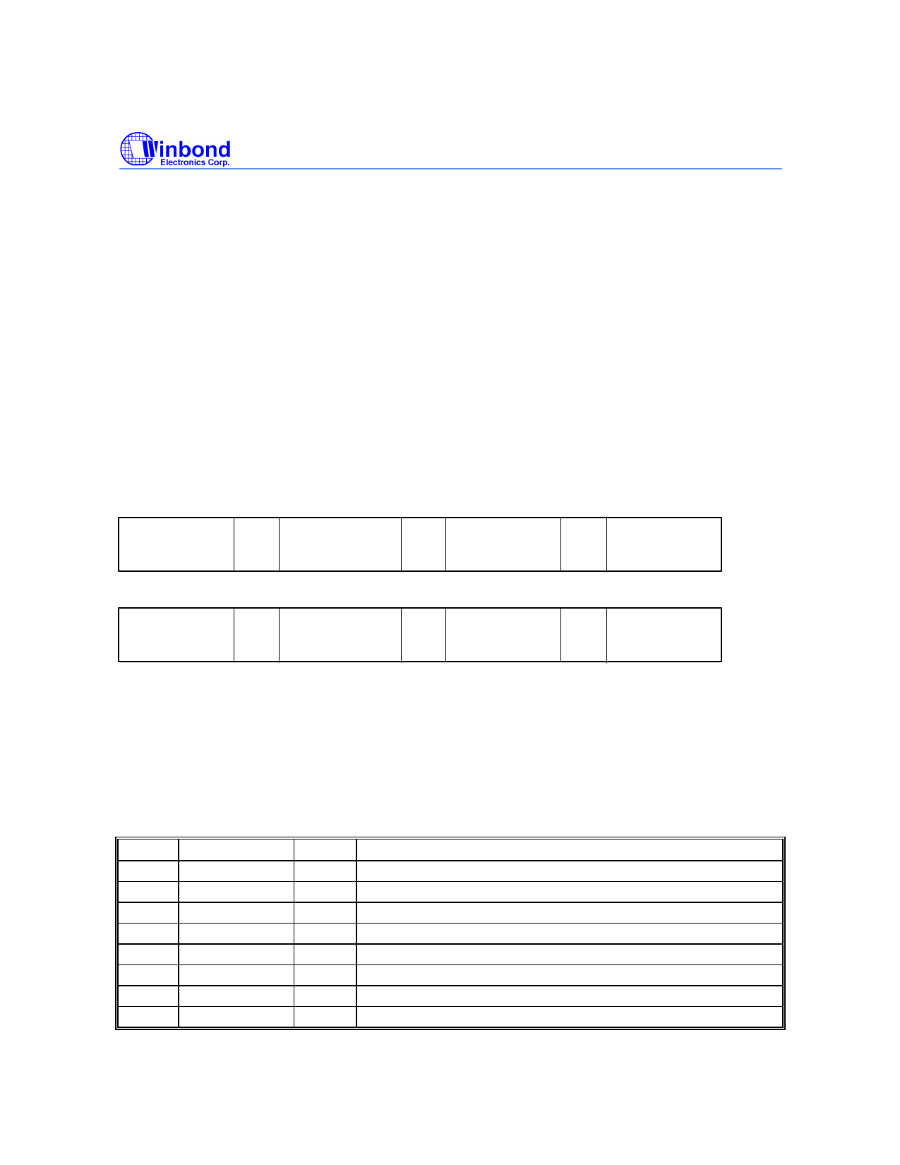
6.2 Serial Control Registers
The Pin column lists the affected pin number and the @PowerUp column gives the state at true
power up. Registers are set to the values shown only on true power up. "Command Code" byte and
"Byte Count" byte must be sent following the acknowledge of the Address Byte. Although the data
(bits) in these two bytes are considered "don't care", they must be sent and will be acknowledge. After
that, the below described sequence (Register 0, Register 1, Register 2, ....) will be valid and
acknowledged.
6.2.1 Register 0: (1 = Active, 0 = Inactive)
BIT @POWERUP PIN
DESCRIPTION
7
1
11 SDRAM5 (Active/Inactive)
6
1
10 SDRAM4 (Active/Inactive)
5
-
- Reserved
4
-
- Reserved
3
1
7 SDRAM3 (Active/Inactive)
2
1
6 SDRAM2 (Active/Inactive)
1
1
3 SDRAM1 (Active/Inactive)
0
1
2 SDRAM0 (Active/Inactive)
Publication Release Date: March 1999
-3-
Revision A1
Share Link: 