NJ88C25 Просмотр технического описания (PDF) - Zarlink Semiconductor Inc
Номер в каталоге
Компоненты Описание
Список матч
NJ88C25 Datasheet PDF : 8 Pages
| |||
NJ88C25
CLOCK
1
2
3
4
5
ENABLE
DATA
A6
A5
A4
A3
A2
(17)28 (18)29 (19)30
(M2)R2 (B1)R1 (B0)R0
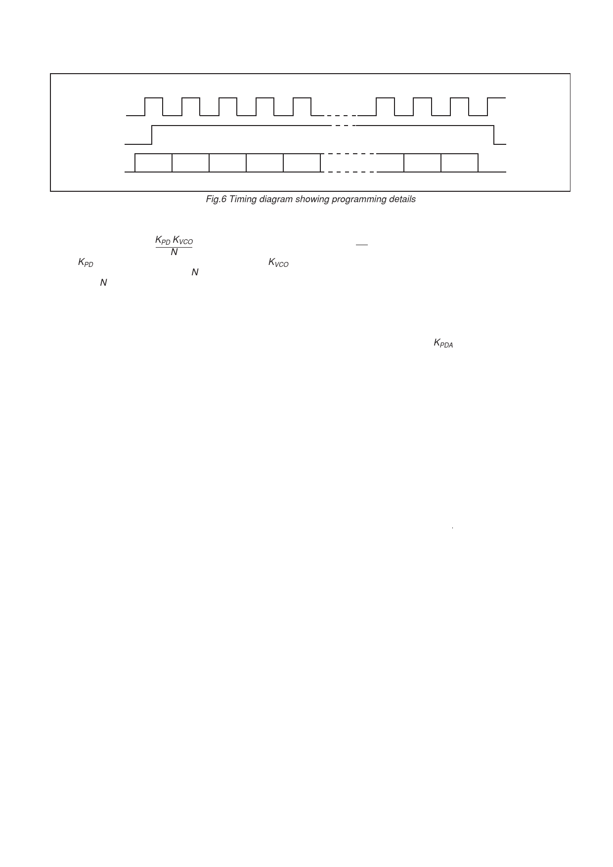
Fig.6 Timing diagram showing programming details
PHASE COMPARATORS
Noise output from a synthesiser loop is related to loop gain:
KPD KVCO
N
where KPD is the phase detector constant (volts/rad), KVCO is
the VCO constant (rad/sec/volt) and N is the overall loop division
ratio. When N is large and the loop gain is low, noise may be
reduced by employing a phase comparator with a high gain.
The sample and hold phase comparator in the NJ88C25 has
a high gain and uses a double sampling technique to reduce
spurious outputs to a low level.
A standard digital phase/frequency detector driving a three-
state output,PDB, provides a ‘coarse’ error signal to enable
fast switching between channels.
The PDB output is active until the phase error is within the
sample and hold phase detector window, when PDB becomes
high impedance. Phase-lock is indicated at this point by a low
level on LD. The sample and hold phase detector provides a
‘fine’ error signal to give further phase adjustment and to hold
the loop in lock. An internally generated ramp, controlled by the
digital output from both the reference and main divider chains,
is sampled at the reference frequency to give the ‘fine’ error
signal, PDA. When in phase lock, this output would be typically
at (VDD2VSS)/2 and any offset from this would be proportional
to phase error.
The relationship between this offset and the phase error is
the phase comparator gain, KPDA, which is programmable with
an external resistor, RB, and a capacitor, CAP. An internal
50pF capacitor is used in the sample and hold comparator.
5
Share Link: 