MCP3901 Просмотр технического описания (PDF) - Microchip Technology
Номер в каталоге
Компоненты Описание
Список матч
MCP3901 Datasheet PDF : 62 Pages
| |||
MCP3901
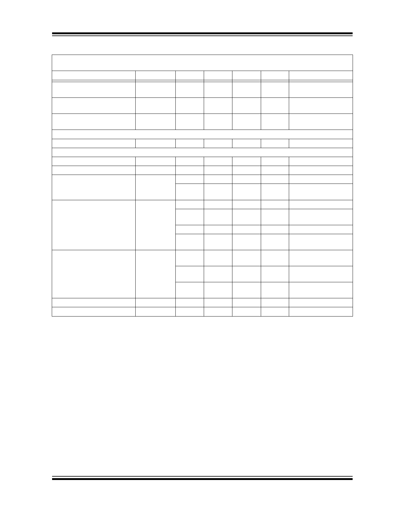
ELECTRICAL CHARACTERISTICS (CONTINUED)
Electrical Specifications: Unless otherwise indicated, AVDD = 4.5 to 5.5V, DVDD = 2.7 to 5.5V; -40°C < TA < +85°C,
MCLK = 4 MHz; PRESCALE = 1; OSR = 64; GAIN = 1; Dithering OFF; VIN = -0.5 dBFS = 333 mVRMS @ 50/60 Hz
Parameters
Symbol
Min Typical Max
Units
Conditions
AC Power Supply Rejection
AC PSRR
—
-77
—
dB AVDD and DVDD = 5V +
1 VPP @ 50/60 Hz
DC Power Supply Rejection
DC PSRR
—
-77
—
dB AVDD and DVDD = 4.5 to
5.5V
DC Common-Mode Rejection
Ratio (Note 2)
CMRR
—
-72
—
dB VCM varies from -1V to
+1V
Oscillator Input
Master Clock Frequency Range
MCLK
1
—
16.384 MHz (Note 8)
Power Specifications
Operating Voltage, Analog
Operating Voltage, Digital
Power On Reset Threshold
AVDD
DVDD
POR
4.5
—
5.5
2.7
3.6
5.5
—
4.2
—
V
V
V (Note 3)
—
4.6
—
-40°C < TA < 125°C,
(Note 3)
Operating Current, Analog
(Note 4)
AIDD
—
2.1
2.8
mA BOOST<1:0> = 00
—
2.1
3.3
mA -40°C < TA < 125°C,
BOOST<1:0> = 00
—
3.8
5.6
mA BOOST<1:0> = 11
—
3.8
7
mA -40°C < TA < 125°C,
BOOST<1:0> = 11
Operating Current, Digital
DIDD
—
0.45
1.0
mA DVDD = 5V,
MCLK = 4 MHz
—
0.25
0.45
mA DVDD = 2.7V,
MCLK = 4 MHz
—
1.2
1.6
mA DVDD = 5V,
MCLK = 8.192 MHz
Shutdown Current, Analog
IDDS,A
—
—
1
µA AVDD pin only (Note 5)
Shutdown Current, Digital
IDDS,D
—
—
1
µA DVDD pin only (Note 5)
Note 1: This specification implies that the ADC output is valid over this entire differential range and that there is no
distortion or instability across this input range. Dynamic performance is specified at -0.5 dB below the
maximum signal range, VIN = -0.5 dBFS @ 50/60 Hz = 353 mVRMS, VREF = 2.4V.
2: See terminology section for definition.
3: This parameter is established by characterization and not 100% tested.
4: For these operating currents, the following bit settings apply: SHUTDOWN<1:0> = 00, RESET<1:0> = 00,
VREFEXT = 0, CLKEXT = 0.
5: For these operating currents, the following Configuration bit settings apply: SHUTDOWN<1:0> = 11,
VREFEXT = 1, CLKEXT = 1.
6: Applies to all gains. Offset error is dependant on PGA gain setting (see Figure 2-19 for typical values).
7: Outside of this range, the ADC accuracy is not specified. An extended input range of ±6V can be applied
continuously to the part with no risk for damage.
8: For proper operation and to keep ADC accuracy, AMCLK should always be in the range of 1 to 5 MHz with
BOOST bits off. With BOOST bits on, AMCLK should be in the range of 1 to 8.192 MHz,
AMCLK = MCLK/PRESCALE. When using a crystal, the CLKEXT bit should be equal to ‘0’.
© 2011 Microchip Technology Inc.
DS22192D-page 5
Share Link: 