MCP3901 Просмотр технического описания (PDF) - Microchip Technology
Номер в каталоге
Компоненты Описание
Список матч
MCP3901 Datasheet PDF : 62 Pages
| |||
MCP3901
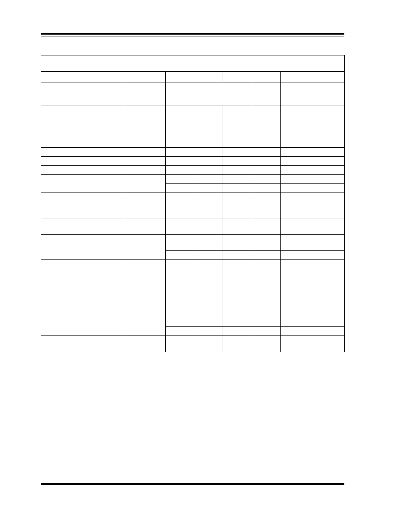
ELECTRICAL CHARACTERISTICS (CONTINUED)
Electrical Specifications: Unless otherwise indicated, AVDD = 4.5 to 5.5V, DVDD = 2.7 to 5.5V; -40°C < TA < +85°C,
MCLK = 4 MHz; PRESCALE = 1; OSR = 64; GAIN = 1; Dithering OFF; VIN = -0.5 dBFS = 333 mVRMS @ 50/60 Hz
Parameters
Symbol
Min Typical Max
Units
Conditions
Output Data Rate
fD
See Table 4-2
ksps fD = DRCLK = DMCLK/
OSR = MCLK/
(4 x PRESCALE x OSR)
Analog Input Absolute Voltage
on CH0+, CH0-, CH1+,
CH1- Pins
CHn+
-1
—
+1
V All analog input
channels, measured to
AGND (Note 7)
Analog Input Leakage Current
AIN
—
—
Differential Input Voltage Range (CHn+ – CHn-) —
1
—
nA (Note 4)
2
—
nA -40°C < TA < 125°C
— 500/GAIN mV (Note 1)
Offset Error (Note 2)
Offset Error Drift
VOS
-3
—
+3
mV (Note 6)
—
3
—
µV/°C From -40°C to +125°C
Gain Error (Note 2)
GE
—
-0.4
—
% G=1
-2.5
—
+2.5
% All Gains
Gain Error Drift
—
1
—
ppm/°C From -40°C to +125°C
Integral Nonlinearity (Note 2)
INL
—
15
—
ppm GAIN = 1,
DITHER = On
Input Impedance
ZIN
350
—
—
kΩ Proportional to
1/AMCLK
Signal-to-Noise and Distortion
SINAD
89
91
—
dB OSR = 256,
Ratio (Notes 2, 3)
DITHER = On
78
79
—
dB
Total Harmonic Distortion
(Notes 2, 3)
THD
—
-104
-102
dB OSR = 256,
DITHER = On
—
-85
-84
dB
Signal-to-Noise Ratio
(Notes 2, 3)
SNR
89
91
—
dB OSR = 256,
DITHER = On
80
81
—
dB
Spurious Free Dynamic Range
(Note 2)
SFDR
—
109
—
dB OSR = 256,
DITHER = On
—
87
—
dB
Crosstalk (50/60 Hz) (Note 2)
CTALK
—
-133
—
dB OSR = 256,
DITHER = On
Note 1:
2:
3:
4:
5:
6:
7:
8:
This specification implies that the ADC output is valid over this entire differential range and that there is no
distortion or instability across this input range. Dynamic performance is specified at -0.5 dB below the
maximum signal range, VIN = -0.5 dBFS @ 50/60 Hz = 353 mVRMS, VREF = 2.4V.
See terminology section for definition.
This parameter is established by characterization and not 100% tested.
For these operating currents, the following bit settings apply: SHUTDOWN<1:0> = 00, RESET<1:0> = 00,
VREFEXT = 0, CLKEXT = 0.
For these operating currents, the following Configuration bit settings apply: SHUTDOWN<1:0> = 11,
VREFEXT = 1, CLKEXT = 1.
Applies to all gains. Offset error is dependant on PGA gain setting (see Figure 2-19 for typical values).
Outside of this range, the ADC accuracy is not specified. An extended input range of ±6V can be applied
continuously to the part with no risk for damage.
For proper operation and to keep ADC accuracy, AMCLK should always be in the range of 1 to 5 MHz with
BOOST bits off. With BOOST bits on, AMCLK should be in the range of 1 to 8.192 MHz,
AMCLK = MCLK/PRESCALE. When using a crystal, the CLKEXT bit should be equal to ‘0’.
DS22192D-page 4
© 2011 Microchip Technology Inc.
Share Link: 