MCP3901 Просмотр технического описания (PDF) - Microchip Technology
Номер в каталоге
Компоненты Описание
Список матч
MCP3901 Datasheet PDF : 62 Pages
| |||
MCP3901
1.0 ELECTRICAL
CHARACTERISTICS
Absolute Maximum Ratings †
VDD ...................................................................................7.0V
Digital inputs and outputs w.r.t. AGND........ -0.6V to VDD +0.6V
Analog input w.r.t. AGND ..................................... ....-6V to +6V
VREF input w.r.t. AGND ............................... -0.6V to VDD +0.6V
Storage temperature .....................................-65°C to +150°C
Ambient temp. with power applied ................-65°C to +125°C
Soldering temperature of leads (10 seconds) ............. +300°C
ESD on the analog inputs (HBM,MM) ................. 7.0 kV, 400V
ESD on all other pins (HBM,MM) ........................ 7.0 kV, 400V
† Notice: Stresses above those listed under “Absolute
Maximum Ratings” may cause permanent damage to the
device. This is a stress rating only and functional operation of
the device at those or any other conditions, above those indi-
cated in the operational listings of this specification, is not
implied. Exposure to maximum rating conditions for extended
periods may affect device reliability.
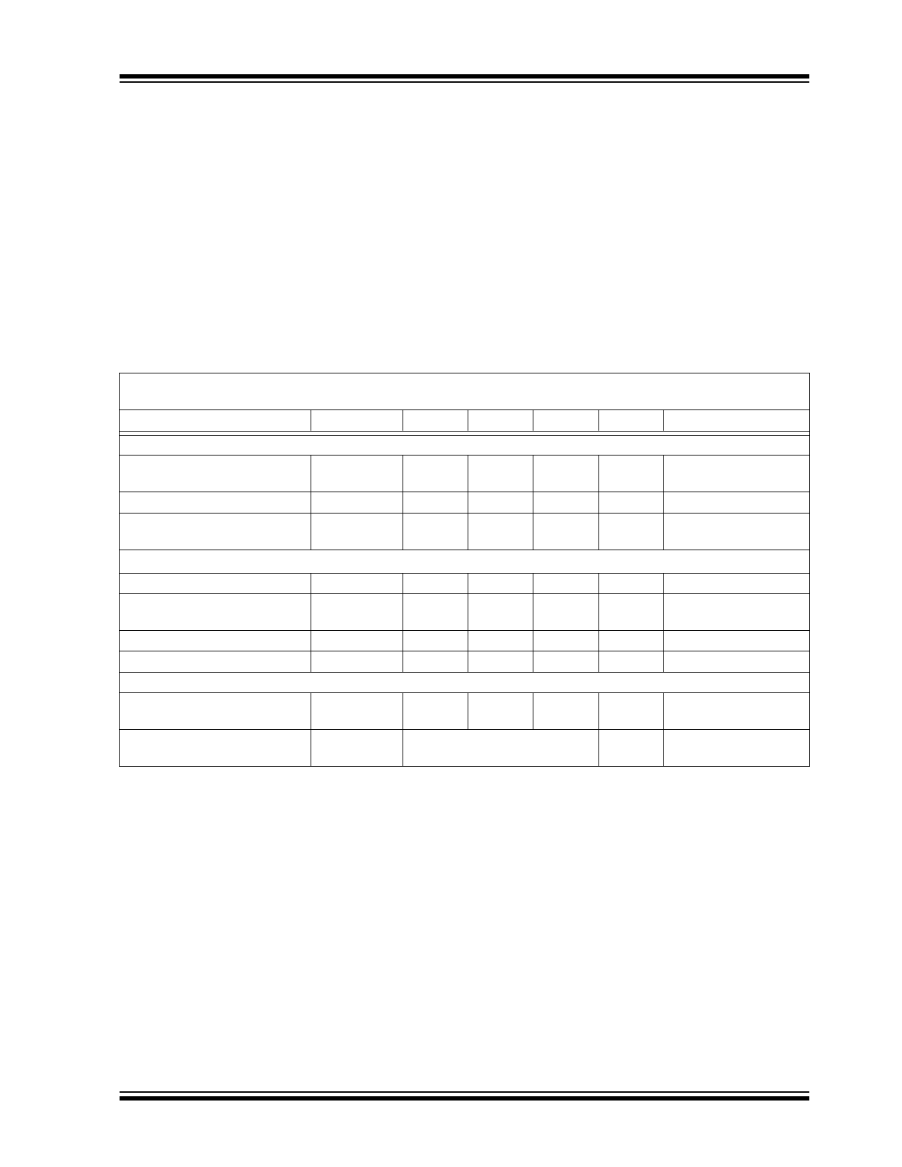
ELECTRICAL CHARACTERISTICS
Electrical Specifications: Unless otherwise indicated, AVDD = 4.5 to 5.5V, DVDD = 2.7 to 5.5V; -40°C < TA < +85°C,
MCLK = 4 MHz; PRESCALE = 1; OSR = 64; GAIN = 1; Dithering OFF; VIN = -0.5 dBFS = 333 mVRMS @ 50/60 Hz
Parameters
Symbol
Min Typical Max
Units
Conditions
Internal Voltage Reference
Internal Voltage Reference
Tolerance
Temperature Coefficient
Output Impedance
VREF
-2%
2.37
+2%
V VREFEXT = 0
TCREF
—
12
—
ppm/°C VREFEXT = 0
ZOUTREF
—
7
—
kΩ AVDD = 5V,
VREFEXT = 0
Voltage Reference Input
Input Capacitance
—
—
10
pF
Differential Input Voltage Range
(VREF+ – VREF-)
VREF
2.2
—
2.6
V
VREF = (VREF+ – VREF-),
VREFEXT = 1
Absolute Voltage on REFIN+ Pin
VREF+
1.9
—
2.9
V VREFEXT = 1
Absolute Voltage on REFIN- Pin
VREF-
-0.3
—
0.3
V
ADC Performance
Resolution (No Missing Codes)
24
—
—
bits OSR = 256
(See Table 5-3)
Sampling Frequency
fS
See Table 4-2
kHz fS = DMCLK = MCLK/
(4 x PRESCALE)
Note 1:
2:
This specification implies that the ADC output is valid over this entire differential range and that there is no
distortion or instability across this input range. Dynamic performance is specified at -0.5 dB below the
maximum signal range, VIN = -0.5 dBFS @ 50/60 Hz = 353 mVRMS, VREF = 2.4V.
See terminology section for definition.
3: This parameter is established by characterization and not 100% tested.
4: For these operating currents, the following bit settings apply: SHUTDOWN<1:0> = 00, RESET<1:0> = 00,
VREFEXT = 0, CLKEXT = 0.
5: For these operating currents, the following Configuration bit settings apply: SHUTDOWN<1:0> = 11,
VREFEXT = 1, CLKEXT = 1.
6: Applies to all gains. Offset error is dependant on PGA gain setting (see Figure 2-19 for typical values).
7: Outside of this range, the ADC accuracy is not specified. An extended input range of ±6V can be applied
continuously to the part with no risk for damage.
8: For proper operation and to keep ADC accuracy, AMCLK should always be in the range of 1 to 5 MHz with
BOOST bits off. With BOOST bits on, AMCLK should be in the range of 1 to 8.192 MHz,
AMCLK = MCLK/PRESCALE. When using a crystal, the CLKEXT bit should be equal to ‘0’.
© 2011 Microchip Technology Inc.
DS22192D-page 3
Share Link: 