MCM72FB8ML7.5R Просмотр технического описания (PDF) - Motorola => Freescale
Номер в каталоге
Компоненты Описание
Список матч
MCM72FB8ML7.5R Datasheet PDF : 20 Pages
| |||
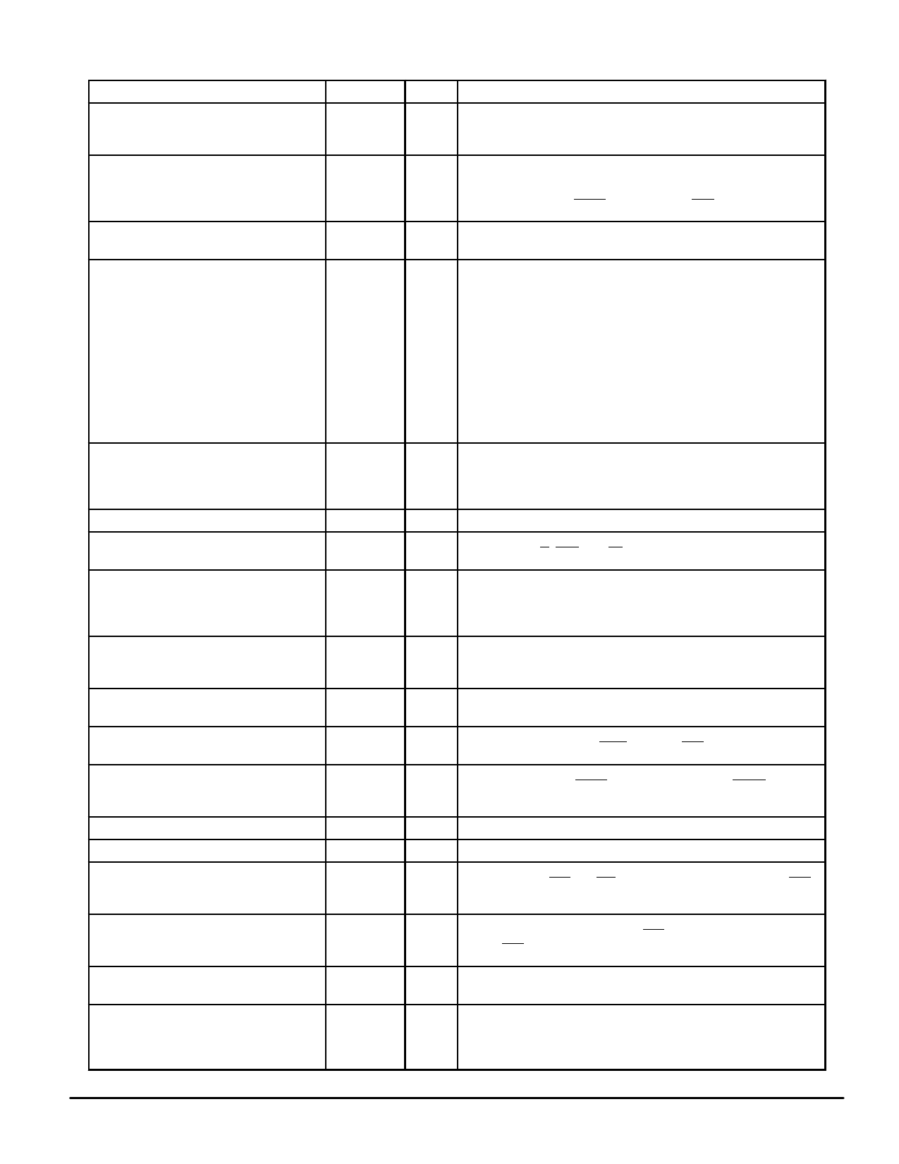
PIN DESCRIPTIONS
Pin Locations
E10
F10
D10
(a) R14, T14, T15, U14, U15, V14, V15,
W14, W15
(b) L14, L15, M14, M15, N14, N15, P14,
P15, R15
(c) E14, F14, F15, G14, G15, H14, H15,
J14, J15
(d) A14, A15, B14, B15, C14, C15, D14,
D15, E15
(e) A5, A6, B5, B6, C5, C6, D5, D6, E5
(f) E6, F5, F6, G5, G6, H5, H6, J5, J6
(g) L5, L6, M5, M6, N5, N6, P5, P6, R5
(h) R6, T5, T6, U5, U6, V5, V6, W5, W6
U13
B10
R10
U7
U10, V10
A7, A8, A9, A11, A12, A13, B7, B8, B9,
B11, B12, B13, V8, V9, V11, V12
L13, K14, K15, J13, J7, K5, K6, L7
(a) (b) (c) (d) (e) (f) (g) (h)
A10
C7
C13
C10
T10
D8, D12, E8, E12, F8, F12, G8,
G12, N8, N12, P8, P12, R8, R12, T8, T12
C8, C9, C11, C12, D7, D13, E7,
E13, F7, F13, G7, G13, H7, H13,
M7, M13, N7, N13, P7, P13, R7,
R13, T7, T13, U8, U9, U11, U12
Symbol
ADSC
ADSP
ADV
DQx
FT
G
K
LBO
SA1, SA0
SA2 – SA17
SBx
SE1
SE2
SE3
SGW
SW
VDD
VDDQ
Type
Input
Input
Input
I/O
Description
Synchronous Address Status Controller: Active low, interrupts any
ongoing burst and latches a new external address. Used to initiate
READ, WRITE, or chip deselect cycle.
Synchronous Address Status Processor: Active low, interrupts any
ongoing burst and latches a new external address. Used to initiate
READ, WRITE, or chip deselect cycle (exception — chip deselect
does not occur when ADSP is asserted and SE1 is high).
Synchronous Address Advance: Increments address count in
accordance with counter type selected (linear/interleaved).
Synchronous Data I/O: “x” refers to the byte being read or written
(byte a, b, c, d, e, f, g, h).
Input
Flow–Through Input: This pin must remain in steady state (this
signal is not registered or latched). It must be tied high or low.
Low — flow–through mode.
High — pipeline mode.
Input Asynchronous Output Enable.
Input Clock: This signal registers the address, data in, and all control
signals except G, LBO, and FT.
Input
Linear Burst Order Input: This pin must remain in steady state (this
signal not registered or latched). It must be tied high or low.
Low — linear burst counter (68K/PowerPC).
High — interleaved burst counter (486/i960/Pentium).
Input
Synchronous Address Inputs: These pins must be wired to the two
LSBs of the address bus for proper burst operation. These inputs
are registered and must meet setup and hold times.
Input Synchronous Address Inputs: These inputs are registered and must
meet setup and hold times.
Input Synchronous Byte Write Inputs: “x” refers to the byte being written
(byte a, b, c, d, e, f, g, h). SGW overrides SBx.
Input
Synchronous Chip Enable: Active low to enable chip.
Negated high–blocks ADSP or deselects chip when ADSC is
asserted.
Input Synchronous Chip Enable: Active high for depth expansion.
Input Synchronous Chip Enable: Active low for depth expansion.
Input
Synchronous Global Write: This signal writes all bytes regardless of
the status of the SBx and SW signals. If only byte write signals SBx
are being used, tie this pin high.
Input
Synchronous Write: This signal writes only those bytes that have
been selected using the byte write SBx pins. If only byte write
signals SBx are being used, tie this pin low.
Supply Core Power Supply.
Supply I/O Power Supply.
MCM72FB8ML MCM72PB8ML
4
MOTOROLA FAST SRAM
Share Link: 