MAX9169ESE Просмотр технического описания (PDF) - Maxim Integrated
Номер в каталоге
Компоненты Описание
Список матч
MAX9169ESE Datasheet PDF : 19 Pages
| |||
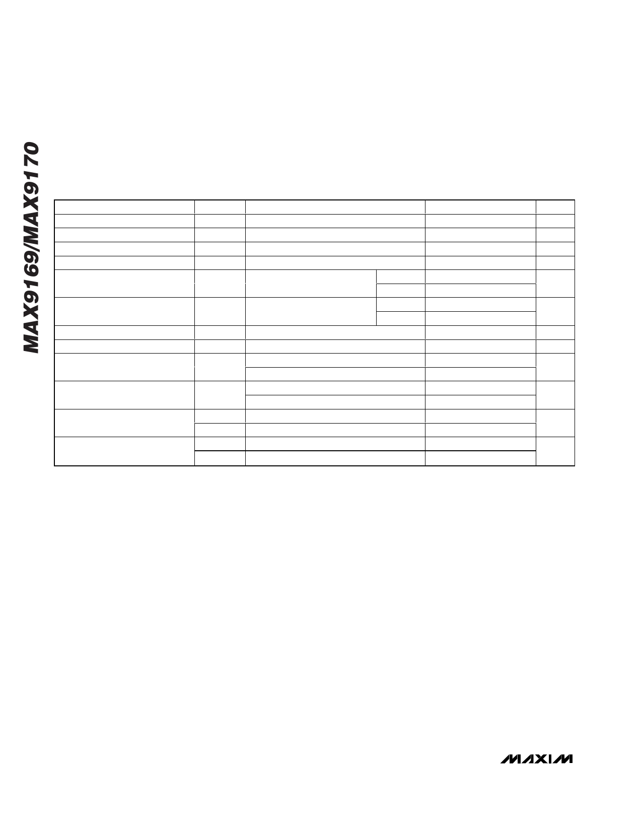
4-Port LVDS and LVTTL-to-LVDS Repeaters
AC ELECTRICAL CHARACTERISTICS
(VCC = 3.0V to 3.6V, RL = 100Ω ±1%, CL = 10pF, EN_ = high, MAX9169 differential input voltage | VID | = 0.15V to 1.2V, LVDS input
common-mode voltage VCM = | VID/2 | to +2.4V - | VID/2 |, TA = -40°C to +85°C, unless otherwise noted. Typical values are at | VID | =
0.2V, VCM = 1.25V, VCC = 3.3V, TA = +25°C for MAX9169. Typical values are at VIN = 0 or VCC, VCC = 3.3V, TA = +25°C for
MAX9170.) (Notes 5, 7, and 8)
PARAMETER
Rise Time
Fall Time
Added Deterministic Jitter
Added Random Jitter
Differential Propagation Delay
High to Low
Differential Propagation Delay
Low to High
Pulse Skew tPLH - tPHL
Pulse Skew tPLH - tPHL
Channel-to-Channel Skew
(Note 12)
Differential Part-to-Part Skew
(Note 13)
Disable Time
Enable Time
SYMBOL
CONDITIONS
MIN
tR
Figures 10–15
0.6
tF
Figures 10–15
0.6
tDJ
(Note 9)
tRJ
(Note 10)
tPHL Figures 10, 11, 13, 14
MAX9169 2.2
MAX9170 1.5
tPLH Figures 10, 11, 13, 14
MAX9169 2.2
MAX9170 1.5
tSKEW
tSK(P)
Figures 10, 11, 13, 14
Figures 10, 12, 13, 15 (Note 11)
tSK(0)
MAX9169, Figures 10, 11, 12
MAX9170, Figures 13, 14, 15
tSK(PP)
MAX9169, Figures 10, 11, 12
MAX9170, Figures 13, 14, 15
tPHZ High to high-Z, Figures 16–19
tPLZ
tPZH
Low to high-Z, Figures 16–19
High-Z to high, Figures 16–19
tPZL High-Z to low, Figures 16–19
TYP MAX UNITS
0.8
1.2
ns
0.8
1.2
ns
110
200
ps
6
8
ps
3.5
4.2
ns
2.6
3.2
3.5
4.2
ns
2.6
3.2
40
250
ps
40
150
ps
25
120
ps
15
100
0.28
1.2
ns
0.19
1.2
11
15
ns
11.8
15
2.3
10
ns
5.8
10
Note 1: Current into a pin is defined as positive. Current out of a pin is defined as negative. All voltages are referenced to ground
except VTH, VTL, VID, VOD, and ∆VOD.
Note 2: Maximum and minimum limits over temperature are guaranteed by design and characterization. Devices are production
tested at TA = +25°C.
Note 3: Signal generator output for IN+, IN-, or single-ended IN: VIN = 0.4 sin(4E6πt) + 0.5.
Note 4: All input pulses are supplied by a generator having the following characteristics: tR or tF ≤ 1ns, pulse repetition rate (PRR) =
0.5 Mpps, pulsewidth = 500 ±10ns.
Note 5: Guaranteed by design and characterization.
Note 6: Signal generator output for OUT+ or OUT-: VIN = 0.4 sin(4E6πt) + 0.5, EN_ = low.
Note 7: CL includes scope probe and test jig capacitance.
Note 8: Signal generator output for differential inputs IN+, IN- (unless otherwise noted): frequency = 50MHz, 49% to 51% duty cycle,
RO = 50Ω, tR = 1.0ns, and tF = 1.0ns (0% to 100%). Signal generator output for single-ended input IN (unless otherwise noted):
frequency = 50MHz, 49% to 51% duty cycle, RO = 50Ω, VIH = VCC, VIL = 0V, tR = 1.0ns, and tF = 1.0ns (0% to 100%).
Note 9: Signal generator output for MAX9169 tDJ: VOH = +1.3V, VOL = +1.1V, data rate = 630Mbps, 223 -1 PRBS, RO = 50Ω,
tR = 1.0ns and tF = 1.0ns (0% to 100%). Signal generator output for MAX9170 tDJ: VOH = VCC, VOL = 0V, data rate =
630Mbps, 223 -1 PRBS, RO = 50Ω, tR = 1.0ns, and tF = 1.0ns (0% to 100%).
Note 10: Signal generator output for MAX9169 tRJ: VOH = +1.3V, VOL = +1.1V, frequency = 315MHz, 50% duty cycle, RO = 50Ω,
tR = 1.0ns, and tF = 1.0ns (0% to 100%). Signal generator output for MAX9170 tRJ: VOH = VCC, VOL = 0V, frequency =
315MHz, 50% duty cycle, RO = 50Ω, tR = 1.0ns, and tF = 1.0ns (0% to 100%).
Note 11: Signal generator output for MAX9169 tSK(P): VOH = +1.4V, VOL = +1.0V, RO = 50Ω, tR = 1.0ns, and tF = 1.0ns (0% to 100%).
Signal generator output for MAX9170 tSK(P): VOH = +3.0, VOL = 0V, RO = 50Ω, tR = 1.0ns, and tF = 1.0ns (0% to 100%).
Note 12: tSK(0) is the magnitude of the time difference between tPLH or tPHL of all drivers of a single device with all of their inputs
connected together.
Note 13: tSK(PP) is the magnitude of the difference in propagation delay times between any specified terminals of two devices when
both devices operate with the same supply voltages, at the same temperature, and have identical packages and test circuits.
4 _______________________________________________________________________________________
Share Link: 