KL5BUDV003 Просмотр технического описания (PDF) - Unspecified
Номер в каталоге
Компоненты Описание
Список матч
KL5BUDV003 Datasheet PDF : 6 Pages
| |||
KL5BUDV003
General Description
USB2.0 to PCI BUS
The Kawasaki KL5KBUDV003 is a high performance device that transfers data between the USB2.0
high-speed BUS and the PCI 33MHz, 32 bit BUS. This 1 chip solution has USB 2.0 transceiver
embedded reducing space and cost. The KL5KBUDV003 is an ideal solution to convert a PCI device to a
USB2.0 Transceiver, HS_SIE USB2.0 Transceiver interface, 4 sets of high-speed bulk packet size
buffers, PCI interface and PCI master 2DMA channel support.
Features
• 33MHz PCI interface
• USB 2.0 standard embedded transceiver.
• 30MHz USB 2.0 SIE BUS for High-Speed SIE
operation
• Double packet buffer - 512x2 HS, 64Bx2 FS
• Internal DMA operation between the High-Speed
SIE and Double Buffer
• High-Speed chirp protocol
• High-Speed/Full-Speed compatibility
• USB basic operation and transaction
control
• Up to 5 endpoints
• PCI interface for Target and Master (2
DMA) modes
• Page and Descriptor DMA Modes
• USB data access by PCI target or DMA
• 0.18u Std cell technology
• Vdd = 3.3V, Ta = 0~70°C
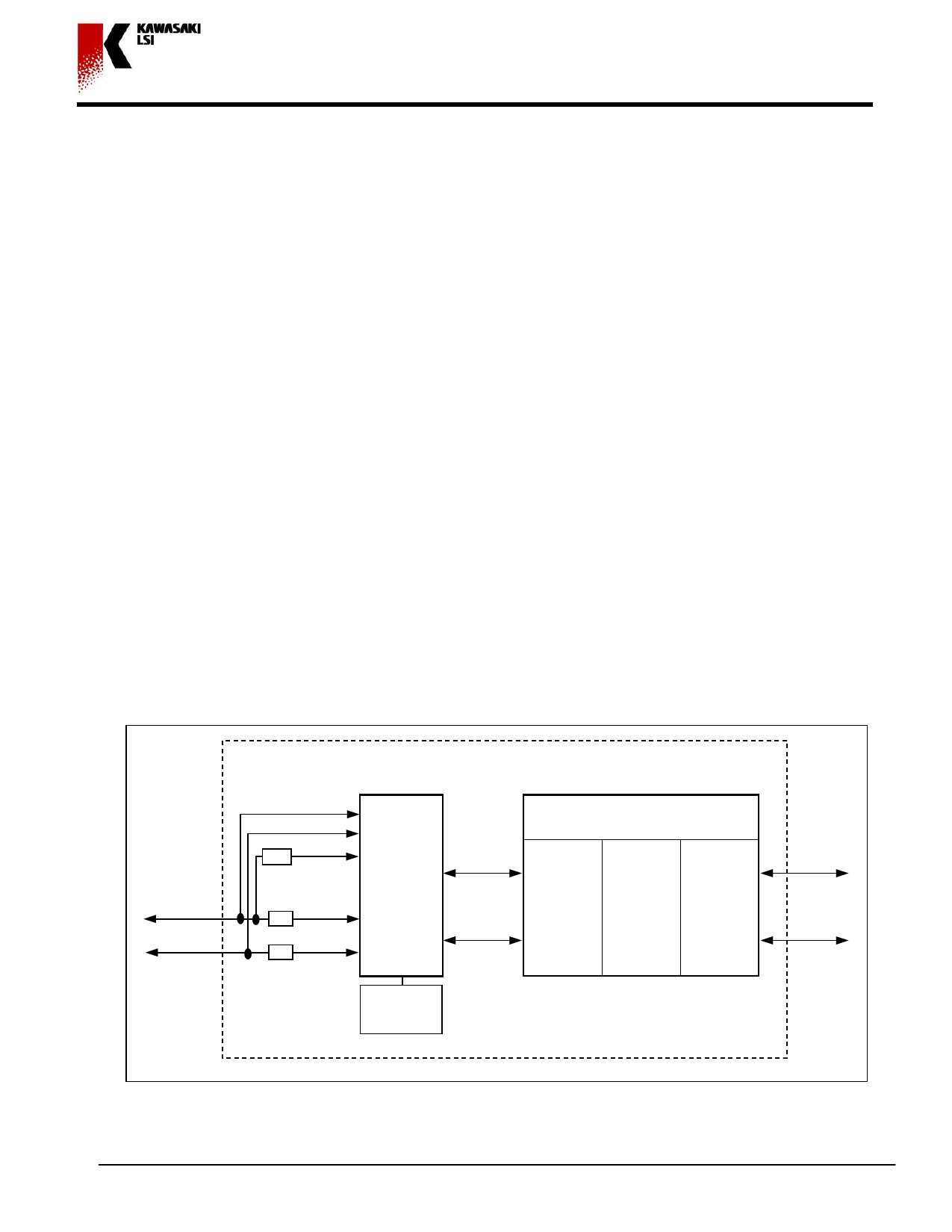
Block Diagram
USB 2.0 D+
USB 2.0 D-
KL5BUDV003
HS D+
HS D-
Rpu RPU_EN
USB 2.0
Transceiver
SIE 16 b
Rs
30 MHz
Rs
USB 2.0 SIE to PCI interface
HS_SIE DBUF
PCI IF
Clock
Generator
PCI 32 b
33 MHz
Kawasaki LSI • 2570 North First Street • Suite 301 • San Jose, CA 95131 • Tel: (408) 570-0555 • Fax: (408) 570-0567 • www.klsi.com Ver. 2.0
1
Share Link: 