IDT723672 Просмотр технического описания (PDF) - Integrated Device Technology
Номер в каталоге
Компоненты Описание
Список матч
IDT723672 Datasheet PDF : 29 Pages
| |||
IDT723652/723662/723672 CMOS SyncBiFIFOTM
2,048 x 36 x 2, 4,096 x 36 x 2 and 8,192 x 36 x 2
mode. IR indicates whether or not the FIFO has available memory locations.
OR shows whether the FIFO has data available for reading or not. It marks the
presence of valid data on the outputs.
Each FIFO has a programmable Almost-Empty flag (AEA and AEB) and a
programmable Almost-Full flag (AFA and AFB). AEA and AEB indicate when
a selected number of words remain in the FIFO memory. AFA and AFB indicate
when the FIFO contains more than a selected number of words.
FFA/IRA, FFB/IRB, AFA and AFB are two-stage synchronized to the port
clock that writes data into its array. EFA/ORA, EFB/ORB, AEA and AEB are two-
stage synchronized to the port clock that reads data from its array. Program-
mable offsets for AEA, AEB, AFA and AFB are loaded by using Port A. Three
default offset settings are also provided. The AEA and AEB threshold can be
COMMERCIAL TEMPERATURE RANGE
set at 8, 16 or 64 locations from the empty boundary and the AFA and AFB
threshold can be set at 8, 16 or 64 locations from the full boundary. All these
choices are made using the FS0 and FS1 inputs during Reset.
Two or more devices may be used in parallel to create wider data paths. If,
at any time, the FIFO is not actively performing a function, the chip will
automatically power down. During the power down state, supply current
consumption (ICC) is at a minimum. Initiating any operation (by activating control
inputs) will immediately take the device out of the power down state.
The IDT723652/723662/723672 are characterized for operation from 0°C
to 70°C. Industrial temperature range (-40°C to +85°C) is available by special
order. They are fabricated using IDT’s high speed, submicron CMOS
technology.
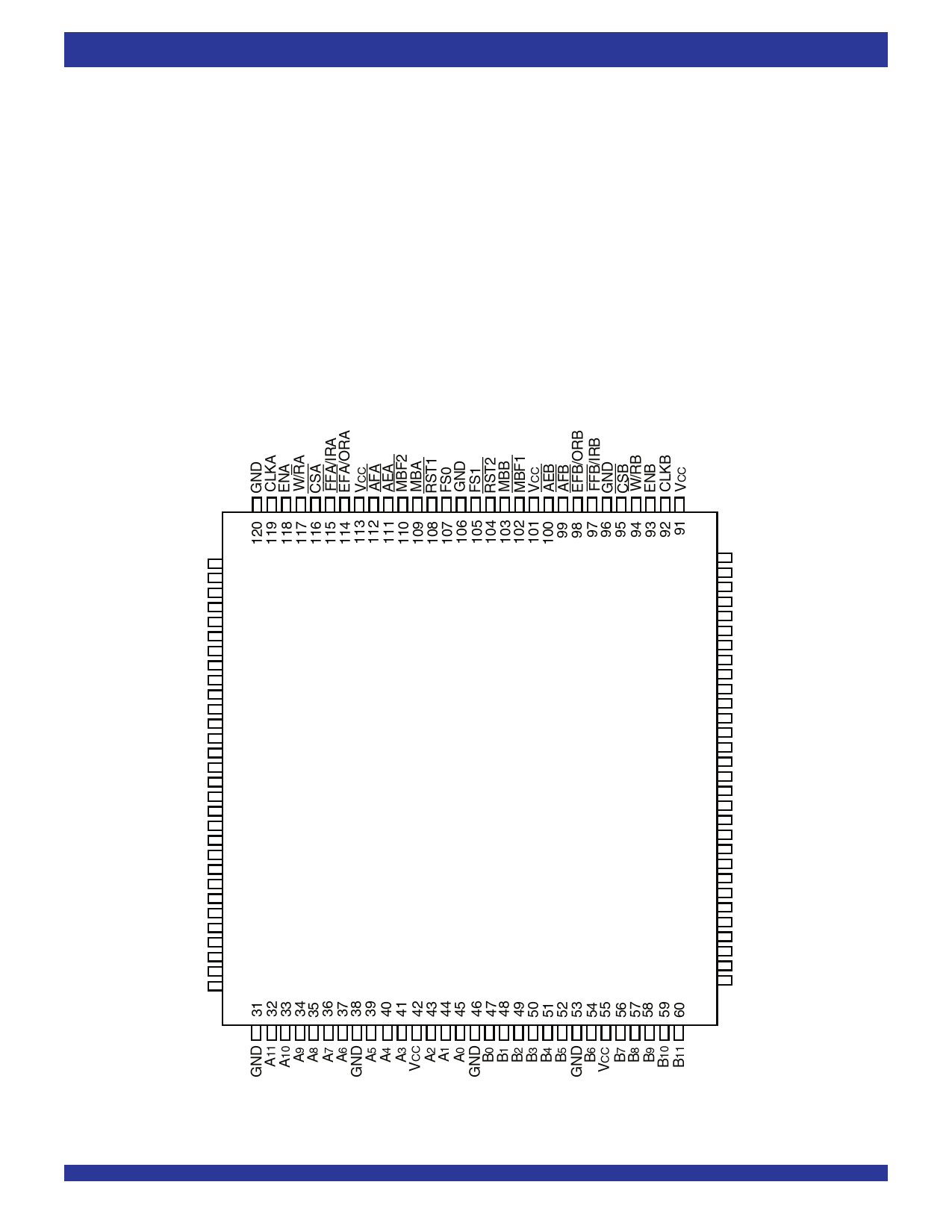
PIN CONFIGURATION (CONTINUED)
A35 1
A34 2
A33 3
A32 4
VCC 5
A31 6
A30 7
GND 8
A29 9
A28 10
A27 11
A26 12
A25 13
A24 14
A23 15
FWFT 16
A22 17
VCC 18
A21 19
A20 20
A19 21
A18 22
GND 23
A17 24
A16 25
A15 26
A14 27
A13 28
VCC 29
A12 30
TQFP (PN120-1, order code: PF)
TOP VIEW
3
90 B35
89 B34
88 B33
87 B32
86 GND
85 B31
84 B30
83 B29
82 B28
81 B27
80 B26
79 VCC
78 B25
77 B24
76 GND
75 B23
74 B22
73 B21
72 B20
71 B19
70 B18
69 GND
68 B17
67 B16
66 VCC
65 B15
64 B14
63 B13
62 B12
61 GND
5609 drw 03
Share Link: 