RF2905 Просмотр технического описания (PDF) - RF Micro Devices
Номер в каталоге
Компоненты Описание
Список матч
RF2905 Datasheet PDF : 22 Pages
| |||
RF2905
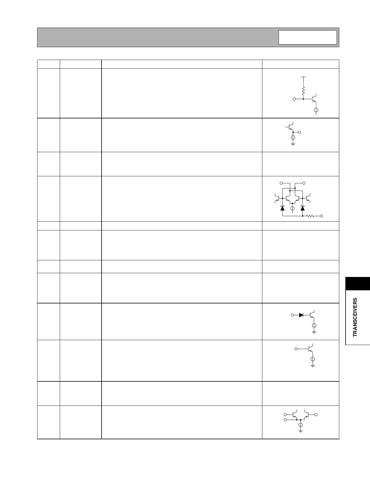
Pin Function Description
Interface Schematic
27 DEMOD IN This pin is the input to the FM demodulator. This pin is NOT AC cou-
pled. Therefore, a DC blocking capacitor is required on this pin to avoid
shorting the demodulator input with the LC tank. A ceramic discrimina-
tor or DC blocked LC tank resonant at the IF should be connected to
this pin.
VCC
DEMOD IN
10 kΩ
28
IF2 OUT Balanced IF output from the 60dB limiting amplifier strip. This pin is
intended to be connected to pin 27 through a 4pF (suggested) capaci-
tor and an FM discriminator circuit.
IF2 OUT
29
VCC6
This pin is used is supply DC bias to the second IF amplifier, Demodu-
lator and Data Slicer. An IF bypass capacitor should be connected
directly to this pin and returned to ground. A 10nF capacitor is recom-
mended for 10.7MHz IF applications.
30
RESNTR+
This port is used to supply DC voltage to the VCO as well as to tune the
center frequency of the VCO. Equal value inductors should be con-
ESNTR+
nected to this pin and pin 31 although a small imbalance can be used
to tune in the proper frequency range.
31
RESNTR- See RESNTR+ description.
See pin 30.
32
VCC2
This pin is used is supply DC bias to the VCO, prescaler, and PLL. An
RF bypass capacitor should be connected directly to this pin and
returned to ground. A 22pF capacitor is recommended for 915MHz
applications. A 68pF capacitor is recommended for 433MHz applica-
tions.
33
GND4
GND4 is the ground shared on chip by the VCO, prescaler, and PLL
electronics.
34
MOD IN FM analog or digital modulation can be imparted to the VCO through See pin 30.
this pin. The VCO varies in accordance to the voltage level presented
to this pin. To set the deviation to a desired level, a voltage divider refer-
enced to Vcc is the recommended. This deviation is also dependent
upon the overall capacitance of the external resonant circuit.
35
DIV CTRL This pin is used to select the desired prescaler divisor. A logic high
(DIVCTRL>2.0V) selects the 64/65 divisor. A logic low
(DIVCTRL<1.0V) selects the 128/129 divisor.
DIV CTL
RESNTR-
4 kΩ
MOD IN
11
36 MOD CTRL This pin is used to select the prescaler modulus. A logic high (MOD
CTRL>2.0V) selects 64 or 128 for the prescaler divisor. A logic low
(MOD CTRL<1.0V) selects 65 or 129 for the prescaler divisor.
Due to design timing constraints, the prescaler in the divide by 65 or
129 modes has a limited frequency range for accurate operation.
These two modes are not recommended for use from 400MHz to
460 MHz.
MOD CTL
37
OSC SEL A logic high (OSC SEL>2.0V) applied to this pin powers on reference
oscillator 2 and powers down reference oscillator 1. A logic low (OSC
SEL<1.0V) applied to this pin powers on reference oscillator 1 and
powers down reference oscillator 2.
38
OSC B2 This pin is connected directly to the reference oscillator 2 transistor
base. The intended reference oscillator configuration is a modified Col- OSC B1
pitts.
OSC E
OSC B2
Rev B11 010516
11-59
Share Link: 