DS1073 Просмотр технического описания (PDF) - Dallas Semiconductor -> Maxim Integrated
Номер в каталоге
Компоненты Описание
Список матч
DS1073 Datasheet PDF : 18 Pages
| |||
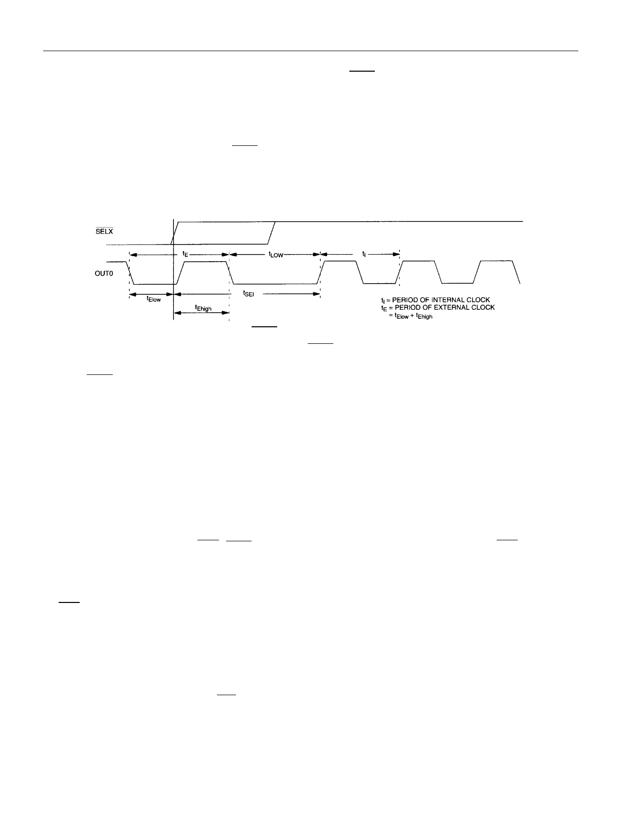
FROM EXTERNAL TO INTERNAL CLOCK
DS1073
This is accomplished by a low to high transition on the SELX pin. In this case the switch is level
triggered, to allow for the possibility of a clock signal not being present at OSCIN. Note therefore, that if
a constant high-level signal is applied to OSCIN it will not be possible to switch over to the internal
reference. (Level triggering was not employed for the switch from internal to external reference as this
approach is slower and the internal clock may be running at a much higher frequency than the maximum
allowed external clock rate). When SELX is high and a low level is sensed on EXTCLK, OUT0 will be
held low until a falling edge occurs on INTCLK, then the next rising edge of INTCLK will be routed
through to OUT0.
Figure 8
Depending on the relative timing of the SELX signal and the external clock, there may be up to one full
tEhigh period on the output after the rising edge of SELX . Then, the “low” time (tLOW) between output
pulses will be dependent on the relative timing between tI and tE. The time interval between the falling
edge of SELX and the first rising edge of the externally derived clock is tSIE. Approximate maximum and
minimum values of these parameters are:
tLOW (min) = tI/2
tLOW (max) = 3tI/2 + tElow
tSIE (min) = tI/2
tSIE (max) = 3tI/2 + tEhigh
NOTE:
In each case there will be a small additional delay due to internal propagation delays.
POWER-DOWN CONTROL
If the PDN bit is set to 1, the PDN / SELX pin can be used to power-down the device. If PDN is high the
device will run normally.
POWER-DOWN
If PDN is taken low a power-down sequence is initiated. The “Enabling Sequencer” is used to execute
events in the following sequence:
1. Disable OUT (same sequence as when OE is used) and reset N counters.
2. When OUT is low, switch OUT to high-impedance state.
3. Disable MCLK (and OUT0 if EN0 bit = 0), switch OUT0 to high impedance state.
4. Disable internal oscillator and OSCIN buffer.
8 of 18
Share Link: 