CY7C1335 Просмотр технического описания (PDF) - Cypress Semiconductor
Номер в каталоге
Компоненты Описание
Список матч
CY7C1335 Datasheet PDF : 15 Pages
| |||
PRELIMINARY
CY7C1335
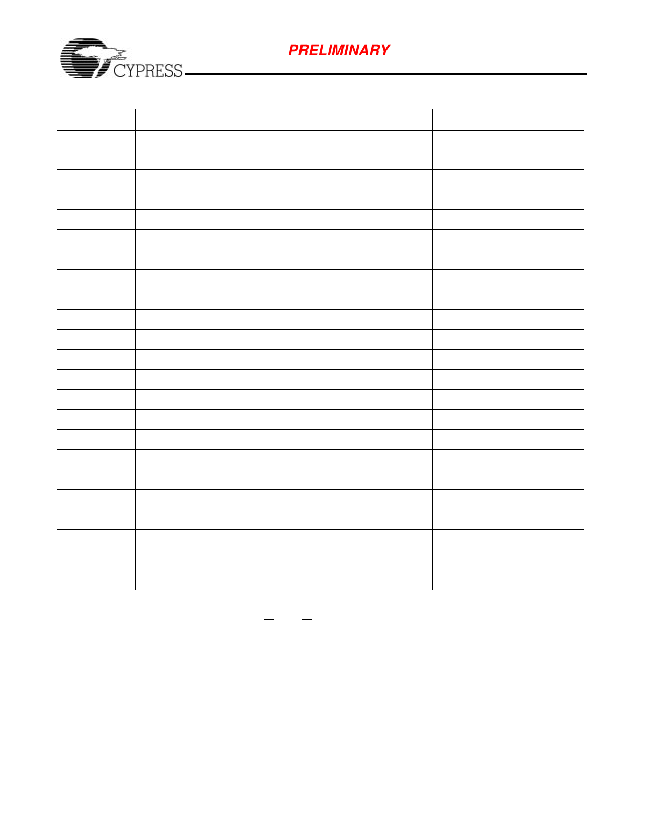
Cycle Descriptions[1,2,3]
Next Cycle Add. Used ZZ
Unselected
None
L
CE3 CE2 CE1 ADSP ADSC ADV OE
X
X
1
X
0
X
X
Unselected
None
L
1
X
0
0
X
X
X
Unselected
None
L
X
0
0
0
X
X
X
Unselected
None
L
1
X
0
1
0
X
X
Unselected
None
L
X
0
0
1
0
X
X
Begin Read
External
L
0
1
0
0
X
X
X
Begin Read
External
L
0
1
0
1
0
X
X
Continue Read Next
L
X
X
X
1
1
0
1
Continue Read Next
L
X
X
X
1
1
0
0
Continue Read Next
L
X
X
1
X
1
0
1
Continue Read Next
L
X
X
1
X
1
0
0
Suspend Read Current
L
X
X
X
1
1
1
1
Suspend Read Current
L
X
X
X
1
1
1
0
Suspend Read Current
L
X
X
1
X
1
1
1
Suspend Read Current
L
X
X
1
X
1
1
0
Begin Write
Current
L
X
X
X
1
1
1
X
Begin Write
Current
L
X
X
1
X
1
1
X
Begin Write
External
L
0
1
0
1
0
X
X
Continue Write Next
L
X
X
X
1
1
0
X
Continue Write Next
L
X
X
1
X
1
0
X
Suspend Write Current
L
X
X
X
1
1
1
X
Suspend Write Current
L
X
X
1
X
1
1
X
ZZ “sleep”
None
H
X
X
X
X
X
X
X
Notes:
1. X=Don't Care, 1=HIGH, 0=LOW.
2. Write is defined by BWE, BW[3:0], and GW. See write table.
3. The DQ pins are controlled by the current cycle and the OE signal. OE is asynchronous and is not sampled with the clock.
DQ
Hi-Z
Hi-Z
Hi-Z
Hi-Z
Hi-Z
Hi-Z
Hi-Z
Hi-Z
DQ
Hi-Z
DQ
Hi-Z
DQ
Hi-Z
DQ
Hi-Z
Hi-Z
Hi-Z
Hi-Z
Hi-Z
Hi-Z
Hi-Z
Hi-Z
Write
X
X
X
X
X
X
read
read
read
read
read
read
read
read
read
write
write
write
write
write
write
write
X
6
Share Link: 