CY7C135-25JC Просмотр технического описания (PDF) - Cypress Semiconductor
Номер в каталоге
Компоненты Описание
Список матч
CY7C135-25JC
Cypress Semiconductor

CY7C135-25JC Datasheet PDF : 12 Pages
| |||
Switching Waveforms (continued)
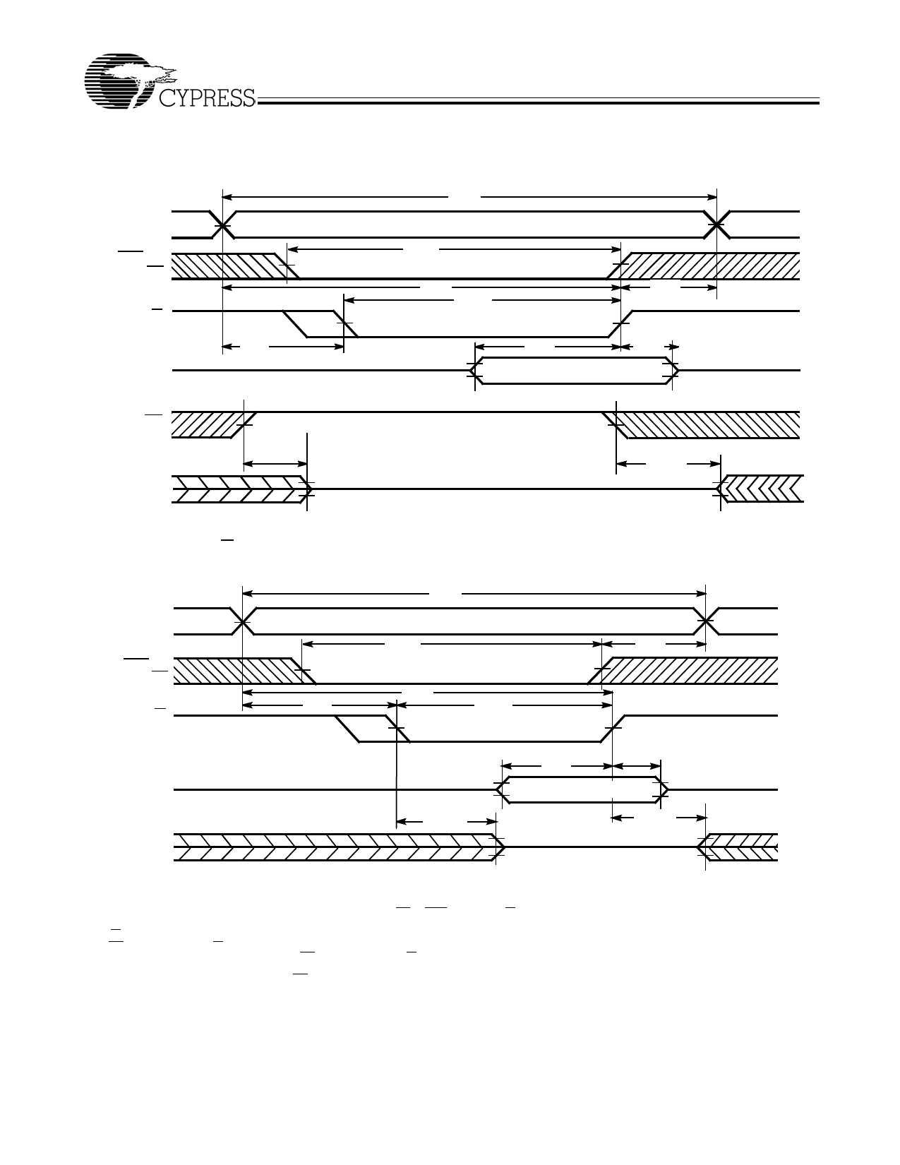
Write Cycle No. 1: OE Three-States Data I/Os (Either Port)[15, 16, 17]
ADDRESS
[10]
SEM
OR CE
R/W
tSA
DATAIN
tWC
tSCE
tAW
tPWE
tSD
DATA VALID
tHA
tHD
CY7C135
CY7C1342
OE
DATAOUT
tHZOE
HIGH IMPEDANCE
tLZOE
Write Cycle No. 2:R/W Three-States Data I/Os (Either Port)[16, 18]
ADDRESS
SEM [10]
OR CE
R/W
tWC
tSCE
tSA
tAW
tPWE
DATAIN
DATAOUT
tHZWE
tHA
tSD
tHD
DATA VALID
tLZWE
HIGH IMPEDANCE
Notes:
15. The internal write time of the memory is defined by the overlap of CE or SEM LOW and R/W LOW. Both signals must be LOW to initiate a write and either signal
can terminate a write by going HIGH. The data input set-up and hold timing should be referenced to the rising edge of the signal that terminates the write.
16. R/W must be HIGH during all address transactions.
17. If OE is LOW during a R/W controlled write cycle, the write pulse width must be the larger of tPWE or (tHZWE + tSD) to allow the I/O drivers to turn off and data to
be placed on the bus for the required tSD. If OE is HIGH during a R/W controlled write cycle (as in this example), this requirement does not apply and the write
pulse can be as short as the specified tPWE.
18. Data I/O pins enter high-impedance when OE is held LOW during write.
Document #: 38-06038 Rev. *C
Page 7 of 12
Share Link: