CY7C1339B-166 Просмотр технического описания (PDF) - Cypress Semiconductor
Номер в каталоге
Компоненты Описание
Список матч
CY7C1339B-166 Datasheet PDF : 17 Pages
| |||
CY7C1339B
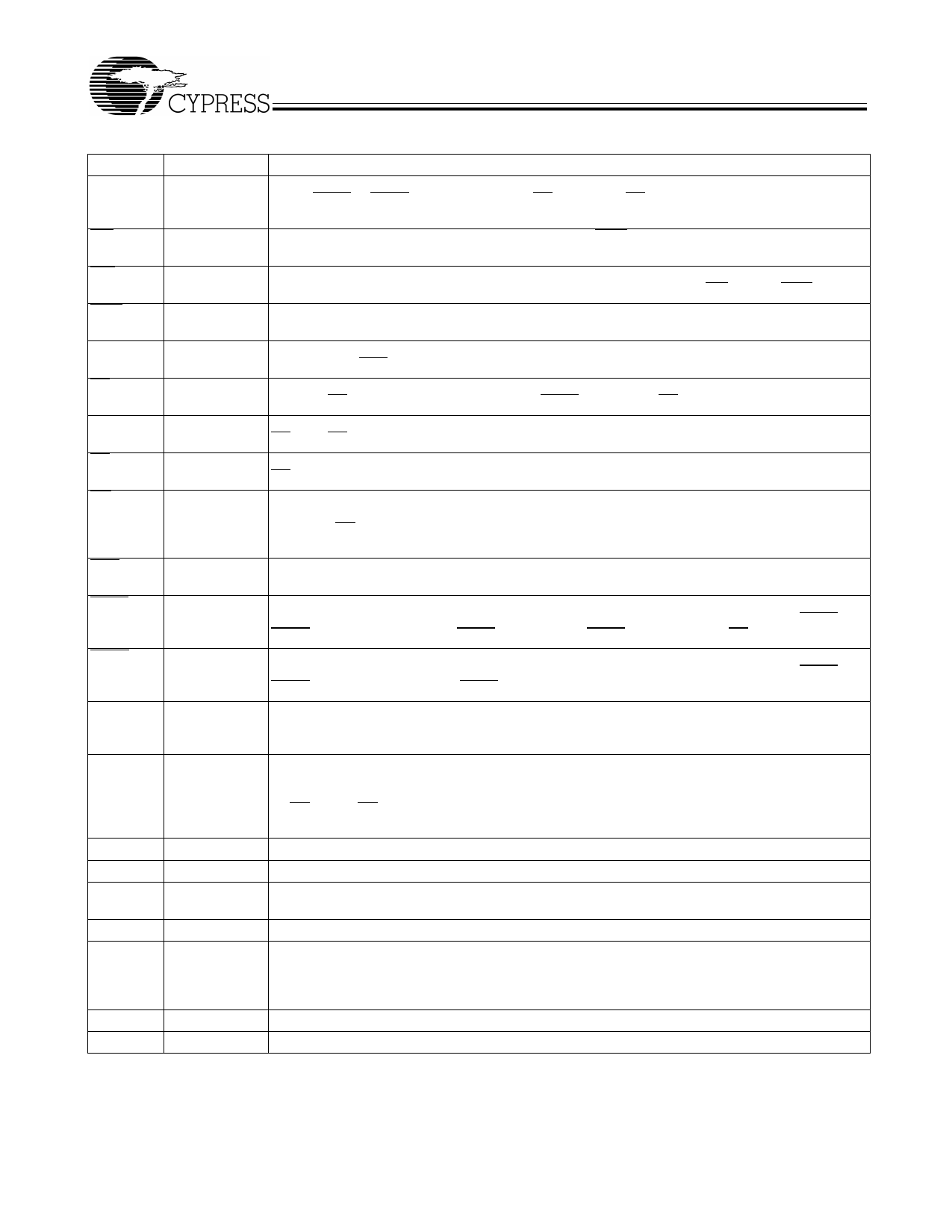
Pin Definitions
Pin Name
A[16:0]
BW[3:0]
GW
BWE
CLK
CE1
CE2
CE3
OE
ADV
ADSP
ADSC
ZZ
DQ[31:0]
VDD
VSS
VDDQ
VSSQ
MODE
NC
DNU
I/O
Pin Description
Input-
Address Inputs used to select one of the 64K address locations. Sampled at the rising edge of the
Synchronous CLK if ADSP or ADSC is active LOW, and CE1, CE2, and CE3 are sampled active. A[1:0] feed the
two-bit counter.
Input-
Byte Write Select Inputs, active LOW. Qualified with BWE to conduct byte writes to the SRAM.
Synchronous Sampled on the rising edge of CLK.
Input-
Synchronous
Input-
Synchronous
Global Write Enable Input, active LOW. When asserted LOW on the rising edge of CLK, a global
Write is conducted (ALL bytes are written, regardless of the values on BW[3:0] and BWE).
Byte Write Enable Input, active LOW. Sampled on the rising edge of CLK. This signal must be
asserted LOW to conduct a Byte Write.
Input-Clock Clock Input. Used to capture all synchronous inputs to the device. Also used to increment the burst
counter when ADV is asserted LOW, during a burst operation.
Input-
Chip Enable 1 Input, active LOW. Sampled on the rising edge of CLK. Used in conjunction with
Synchronous CE2 and CE3 to select/deselect the device. ADSP is ignored if CE1 is HIGH.
Input-
Chip Enable 2 Input, active HIGH. Sampled on the rising edge of CLK. Used in conjunction with
Synchronous CE1 and CE3 to select/deselect the device.
Input-
Chip Enable 3 Input, active LOW. Sampled on the rising edge of CLK. Used in conjunction with
Synchronous CE1 and CE2 to select/deselect the device.
Input-
Output Enable, Asynchronous Input, active LOW. Controls the direction of the I/O pins. When LOW,
Asynchronous the I/O pins behave as outputs. When deserted HIGH, I/O pins are three-stated, and act as input
data pins. OE is masked during the first clock of a Read cycle when emerging from a deselected
state.
Input-
Advance Input Signal, sampled on the rising edge of CLK. When asserted, it automatically incre-
Synchronous ments the address in a burst cycle.
Input-
Synchronous
Input-
Synchronous
Address Strobe from Processor, sampled on the rising edge of CLK. When asserted LOW, A[16:0]
is captured in the address registers. A[1:0] are also loaded into the burst counter. When ADSP and
ADSC are both asserted, only ADSP is recognized. ASDP is ignored when CE1 is deserted HIGH.
Address Strobe from Controller, sampled on the rising edge of CLK. When asserted LOW, A[16:0]
is captured in the address registers. A[1:0] are also loaded into the burst counter. When ADSP and
ADSC are both asserted, only ADSP is recognized.
Input-
ZZ “sleep” Input. This active HIGH input places the device in a non-time-critical “sleep” condition
Asynchronous with data integrity preserved. Leaving ZZ floating or NC will default the device into an active state.
ZZ has an internal pull down.
I/O-
Synchronous
Bidirectional Data I/O Lines. As inputs, they feed into an on-chip data register that is triggered by
the rising edge of CLK. As outputs, they deliver the data contained in the memory location specified
by A[16:0] during the previous clock rise of the Read cycle. The direction of the pins is controlled
by OE. When OE is asserted LOW, the pins behave as outputs. When HIGH, DQ[31:0] are placed
in a three-state condition.
Power Supply Power supply inputs to the core of the device. Should be connected to 3.3V power supply.
Ground Ground for the core of the device. Should be connected to ground of the system.
I/O Power Power supply for the I/O circuitry. Should be connected to a 3.3V or 2.5V power supply.
Supply
I/O Ground Ground for the I/O circuitry. Should be connected to ground of the system.
Input-
Static
Selects Burst Order. When tied to GND selects linear burst sequence. When tied to VDDQ or left
floating selects interleaved burst sequence. This is a strap pin and should remain static during
device operation. When left floating or NC, defaults to interleaved burst order. Mode pin has an
internal pull up.
–
No Connects.
-
Do Not Use pins. These pins could be left floating or tied to GND.
Document #: 38-05141 Rev. *A
Page 4 of 17
Share Link: 