CY7C1339B-166 Просмотр технического описания (PDF) - Cypress Semiconductor
Номер в каталоге
Компоненты Описание
Список матч
CY7C1339B-166 Datasheet PDF : 17 Pages
| |||
CY7C1339B
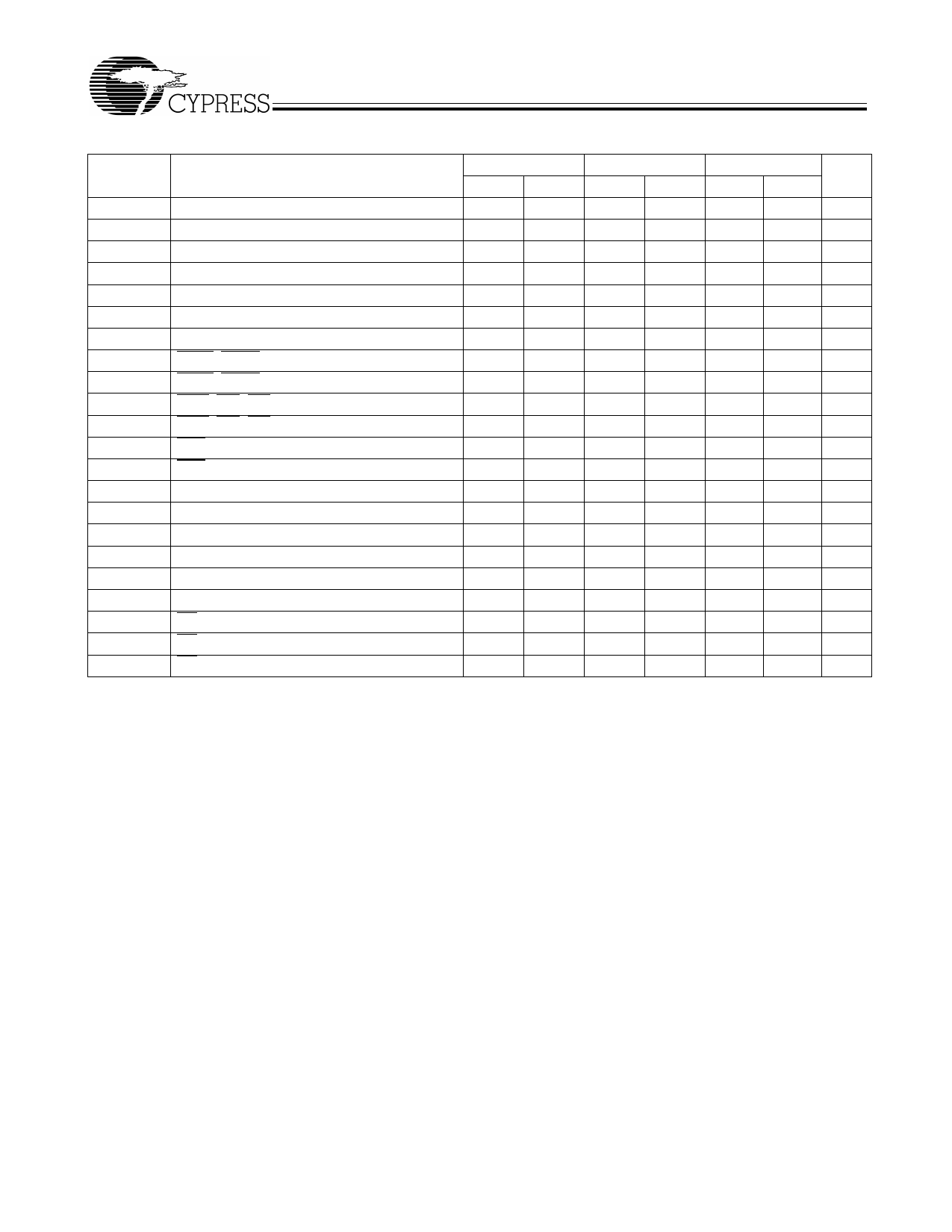
Switching Characteristics Over the Operating Range[10, 12, 13]
-166
-133
-100
Parameter
Description
Min. Max. Min. Max. Min. Max. Unit
tCYC
Clock Cycle Time
6.0
7.5
10
ns
tCH
Clock HIGH
1.7
1.9
3.5
ns
tCL
Clock LOW
1.7
1.9
3.5
ns
tAS
Address Set-Up Before CLK Rise
1.5
1.5
1.5
ns
tAH
Address Hold After CLK Rise
0.5
0.5
0.5
ns
tCO
Data Output Valid After CLK Rise
3.5
4.0
5.5
ns
tDOH
Data Output Hold After CLK Rise
1.5
2.0
2.0
ns
tADS
ADSP, ADSC Set-up Before CLK Rise
2.0
2.5
2.5
ns
tADH
ADSP, ADSC Hold After CLK Rise
0.5
0.5
0.5
ns
tWES
BWE, GW, BW[3:0] Set-up Before CLK Rise 2.0
2.5
2.5
ns
tWEH
BWE, GW, BW[3:0] Hold After CLK Rise
0.5
0.5
0.5
ns
tADVS
ADV Set-Up Before CLK Rise
2.0
2.5
2.5
ns
tADVH
ADV Hold After CLK Rise
0.5
0.5
0.5
ns
tDS
Data Input Set-up Before CLK Rise
1.5
1.5
1.5
ns
tDH
Data Input Hold After CLK Rise
0.5
0.5
0.5
ns
tCES
Chip Select Set-up
2.0
2.5
2.5
ns
tCEH
tCHZ
tCLZ
tEOHZ
tEOLZ
tEOV
Chip Select Hold After CLK Rise
Clock to High-Z[12]
Clock to Low-Z[12]
OE HIGH to Output High-Z[12, 13]
OE LOW to Output Low-Z[12, 13]
OE LOW to Output Valid[12]
0.5
0.5
0.5
ns
3.5
3.5
3.5
ns
0
0
0
ns
3.5
3.5
5.5
ns
0
0
0
ns
3.5
4.0
5.5
ns
Notes:
11. Unless otherwise noted, test conditions assume signal transition time of 3.0/2.5 ns or less, timing reference levels of 1.5/1.25V, input pulse levels of 0 to
3.0/2.5V for 3.3/2.5V VDDQ respectively, and output loading of the specified IOL/IOH and load capacitance. Shown in (a) and (c) of AC test loads diagram.
12. tCHZ, tCLZ, tEOV, tEOLZ, and tEOHZ are specified with a load capacitance of 5 pF as in part (b) of AC Test Loads. Transition is measured ± 200 mv from
steady-state voltage.
13. At any given voltage and temperature, tEOHZ is less than tEOLZ and tCHZ is less than tCLZ.
Document #: 38-05141 Rev. *A
Page 10 of 17
Share Link: 