CMX649 Просмотр технического описания (PDF) - CML Microsystems Plc
Номер в каталоге
Компоненты Описание
Список матч
CMX649 Datasheet PDF : 50 Pages
| |||
ADM Codec
CMX649
20
0
-20
-40
-60
-80
-100
-120
-140
-160
-180
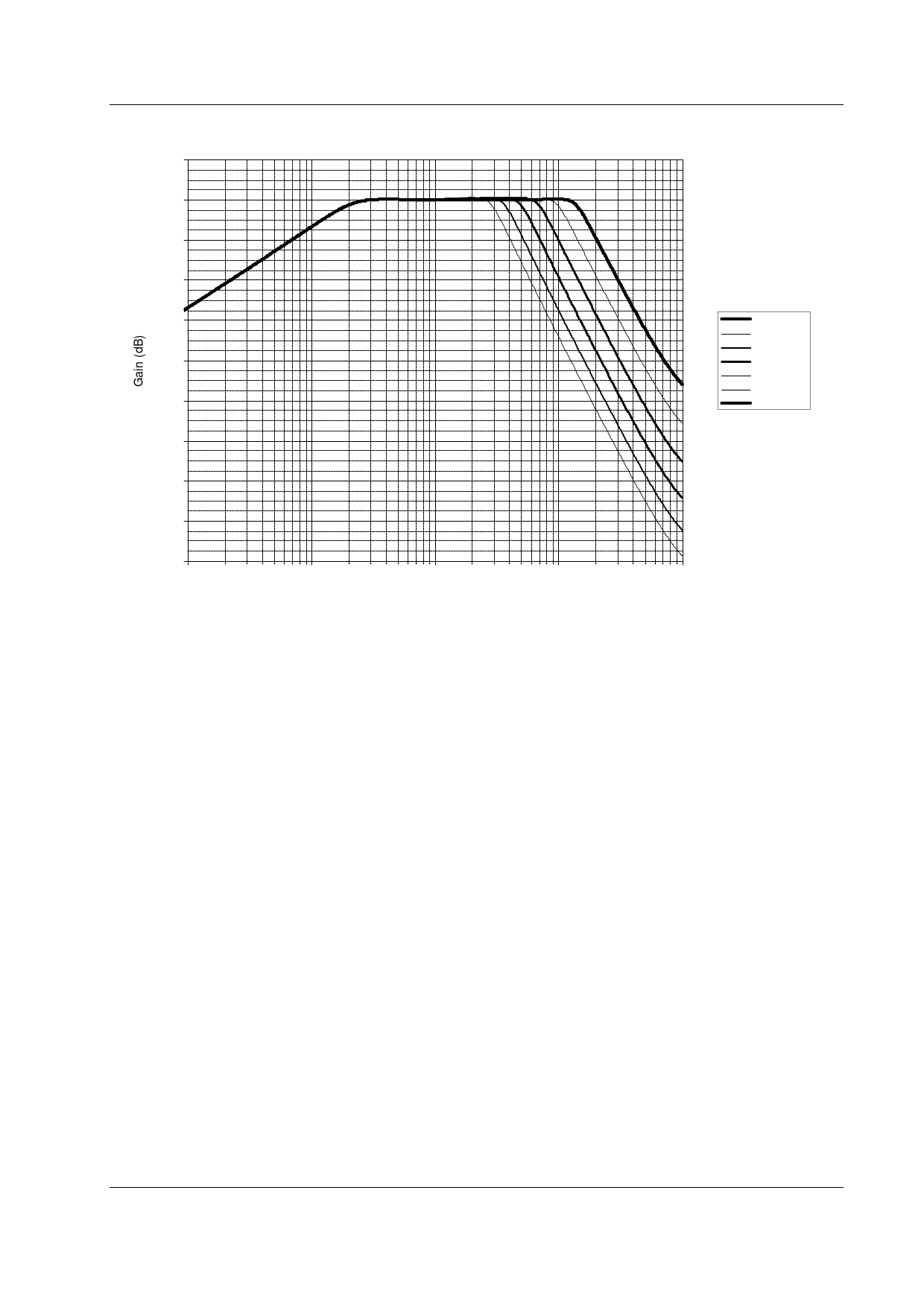
10
B W = 14 . 0 k H z
B W = 10 . 0 k H z
BW=7.0kHz
BW=5.0kHz
BW=3.7kHz
BW=2.9kHz
HPF
100
1,000
10,000
Frequency (Hz)
100,000
Figure 10b Typical Anti-Image Filter Frequency Response
5.1.8 Data Clock Recovery
Data from the RX DATA pin is driven into a comparator to remove amplitude variations. The output of the
comparator is a logic signal that can be inverted by setting the appropriate control bit in the SCRAMBLER
CONTROL Register ($71). Using the output of the comparator, the clock recovery block can be enabled
to generate a phase-locked clock equal to the CVSD data rate, which is used to clock data from the RX
DATA pin into the decoder. The recovered clock frequency is controlled by the CLK DIVIDER CONTROL
Register ($72). If the clock recovery block is bypassed, data must then be applied which is synchronised
to the clock on the RX CLK pin (either internally generated or externally applied).
External ADM rate bit clocks can be used for both the encoder and decoder paths and do not require use
of the clock recovery PLL. Externally applied clocks act directly as the ADM sample clocks and should
be generated with little jitter for best performance. Please note that the maximum usable frequency of
externally applied bit clocks is 1/60th of the frequency of the output of the internal bit clock prescaler.
The clock recovery circuit is normally applied to the decoder. However, it is possible to use the recovered
clock for the encoder section as well. This supports systems where the base unit is using an internal clock
or local external clock for transmit and clock recovery for the decoder clock. The remote unit can then be
configured to use the recovered clock for both encode and decode. Internal data clocks for the encoder
and decoder can also be selected for data input and output control.
5.1.9 Data Scrambler/De-scrambler
The scrambler receives digital data from the encoder. It is implemented with a 10-bit programmable
linear feedback shift register (LFSR) allowing a choice of various maximal length scrambling codes. The
scrambler, also known as a randomizer, provides not only a level of communication security, but may
also help reduce the occurrence of abnormally long strings of 1s or 0s.
© 2003 CML Microsystems Plc
11
D/649/2
Share Link: 