RV5C338A-E2 Просмотр технического описания (PDF) - RICOH Co.,Ltd.
Номер в каталоге
Компоненты Описание
Список матч
RV5C338A-E2
RICOH Co.,Ltd.

RV5C338A-E2 Datasheet PDF : 52 Pages
| |||
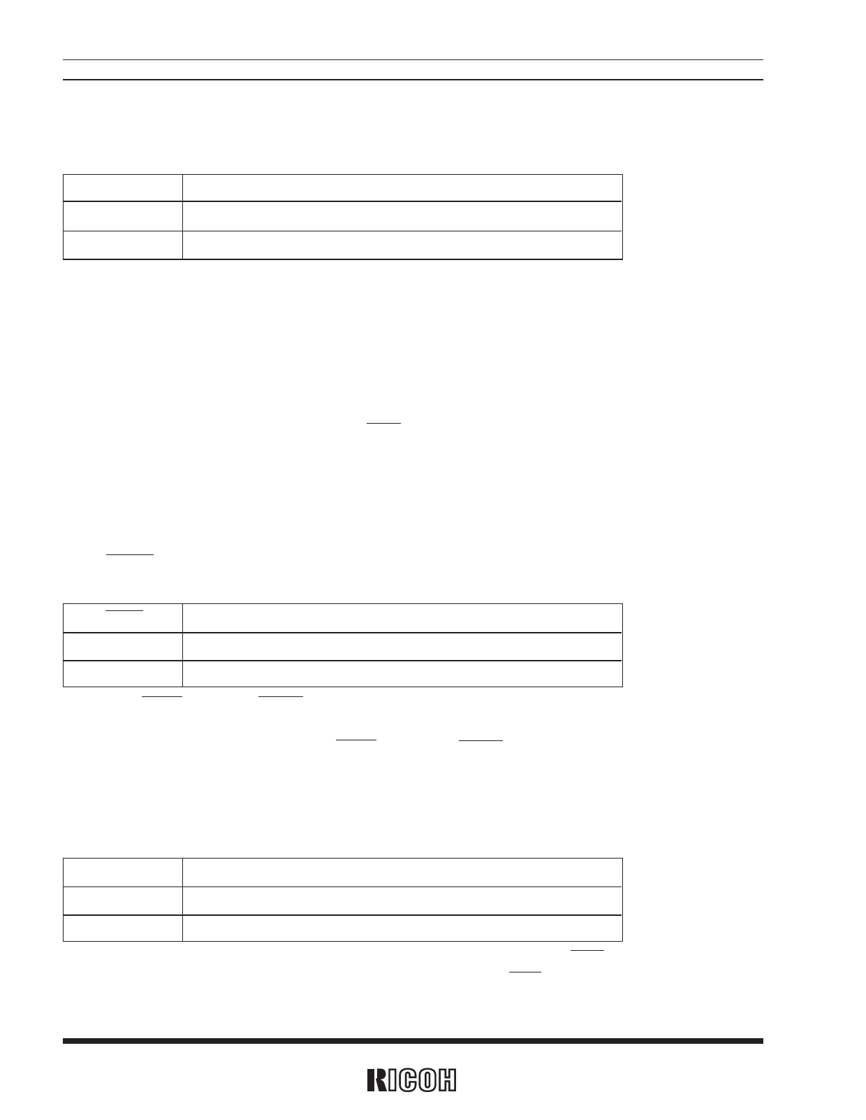
R×5C338A
2.2-4 XSTP
Oscillator Halt Sensing Bit
XSTP
0
1
Description
Sensing a normal condition of oscillation
Sensing a halt of oscillation
(Default setting)
The XSTP bit is for sensing a halt in the oscillation of the crystal oscillator. The oscillation halt sensing circuit
operates only when the CE pin is “L”.
· The XSTP bit will be set to 1 once a halt in the oscillation of the crystal oscillator is caused by such events as pow-
er-on from 0 volts and a drop in supply voltage. The XSTP bit will hold the setting of 1 even after the restart of
oscillation. As such, the XSTP bit can be applied to judge the validity of clock and calendar data after power-on or
a drop in supply voltage.
· When the XSTP bit is set to 1, all bits will be reset to 0 in the oscillation adjustment register, control register 1, and
control register 2, stopping the output from the INTR pin and starting the output of 32.768-kHz clock pulses from
the 32KOUT pin.
(32KOUT output is disabled when CLKC pin is set to low.)
· The XSTP bit accepts only the writing of 0, which restarts the oscillation halt sensing circuit. Conversely, setting
the XSTP bit to 1 causes no event.
2.2-5 CLEN1
32-kHz Clock Output Bit 1
CLEN1
0
Description
Enabling the 32-kHz clock output
(Default setting)
1
Disabling the 32-kHz clock output
Setting the CLEN1 bit or the CLEN2 bit (D4 in control register 1) to 0, and the CLKC pin to high specifies
generating clock pulses with the oscillation frequency of the 32.768-kHz crystal oscillator for output from the
32KOUT pin. Conversely, setting both the CLEN1 bit and the CLEN2 bit to 1 or the CLKC pin to low specifies
disabling (“L”) such output.
2.2-6 CTFG
Periodic Interrupt Flag Bit
CTFG
Description
0
Periodic interrupt output “H” (OFF)
(Default setting)
1
Periodic interrupt output “L” (ON)
The CTFG bit is set to 1 when the periodic interrupt signals are output from the INTR pin (“L”). The CTFG bit
accepts only the writing of 0 in the level mode, which disables (“H”) the INTR pin until it is enabled (“L”) again in
the next interrupt cycle. Conversely, setting the CTFG bit to 1 causes no event.
14
Share Link: