ADP130 Просмотр технического описания (PDF) - Analog Devices
Номер в каталоге
Компоненты Описание
Список матч
ADP130 Datasheet PDF : 20 Pages
| |||
350 mA, Low VIN, Low Quiescent Current,
CMOS Linear Regulator
ADP130
FEATURES
350 mA maximum output current
Input voltage supply range
VBIAS = 2.3 V to 5.5 V
VIN = 1.2 V to 3.6 V
2.3 V < VIN < 3.6 V, VIN can be tied to VBIAS
Very low dropout voltage: 17 mV @ 100 mA load
Low quiescent current: 25 μA @ no load
Low shutdown current: <1 μA
±1% accuracy @ 25°C
Excellent PSRR performance: 70 dB @ 10 kHz
Excellent load/line transient response
Optimized for small 1 μF ceramic capacitors
Current limit and thermal overload protection
Logic controlled enable
5-lead TSOT package
APPLICATIONS
Mobile phones
Digital camera and audio devices
Portable and battery-powered equipment
Post dc-to-dc regulation
GENERAL DESCRIPTION
The ADP130 is a low quiescent current, low dropout linear regu-
lator. It is designed to operate in dual-supply mode with an input
voltage as low as 1.2 V to increase efficiency and provide up to
350 mA of output current. The low 17 mV dropout voltage at
a 100 mA load improves efficiency and allows operation over
a wider input voltage range.
A dual-supply power solution typically improves conversion
efficiency over a single-supply solution because the higher VBIAS
supply powers the part, and the lower VIN supply delivers current
to the load. The power dissipated in the device is thereby reduced.
The ADP130 is optimized for stable operation with small 1 μF
ceramic output capacitors. The ADP130 delivers good transient
performance with minimal board area.
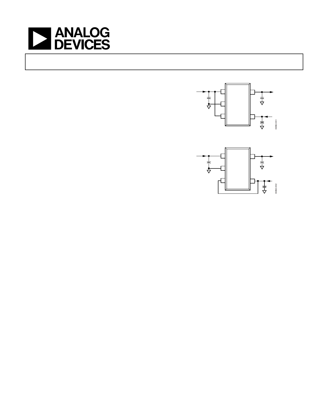
TYPICAL APPLICATION CIRCUITS
VIN = 1.8V
+
1µF
1 VIN
VOUT = 1.2V
VOUT 5
ADP130
+
1µF
2 GND
3 EN
VBIAS
VBIAS = 3.6V
4
+
1µF
Figure 1.
VIN = 2.8V
+
1µF
1 VIN
VOUT = 1.8V
VOUT 5
ADP130
+
1µF
2 GND
3 EN
VBIAS 4
VBIAS = 5V
+
1µF
Figure 2.
The ADP130 is available in the following 31 fixed output voltage
options:
• 0.80 V to 2.00 V in 50 mV steps
• 1.875 V, 2.25 V, 2.50 V, 2.775 V, 2.80 V, and 3.0 V
The ADP130 has a typical internal soft start time of 200 μs. Short-
circuit protection and thermal overload protection circuits
prevent damage in adverse conditions. The ADP130 is available
in a tiny 5-lead TSOT package for the smallest footprint solution to
meet a variety of portable power applications.
Rev. 0
Information furnished by Analog Devices is believed to be accurate and reliable. However, no
responsibility is assumed by Analog Devices for its use, nor for any infringements of patents or other
rights of third parties that may result from its use. Specifications subject to change without notice. No
license is granted by implication or otherwise under any patent or patent rights of Analog Devices.
Trademarks and registered trademarks are the property of their respective owners.
One Technology Way, P.O. Box 9106, Norwood, MA 02062-9106, U.S.A.
Tel: 781.329.4700
www.analog.com
Fax: 781.461.3113
©2008 Analog Devices, Inc. All rights reserved.
Share Link: 