5962-9461201HMX Просмотр технического описания (PDF) - Aeroflex Corporation
Номер в каталоге
Компоненты Описание
Список матч
5962-9461201HMX Datasheet PDF : 20 Pages
| |||
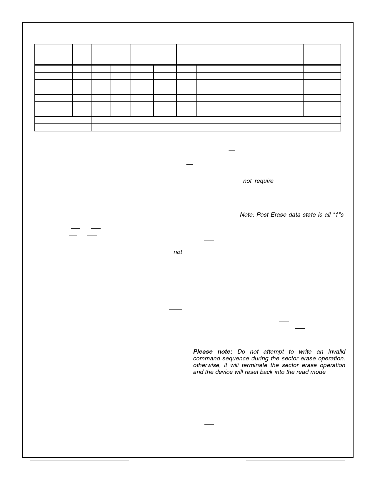
Table 3 — Commands Definitions
Command
Sequence
Bus
Write First Bus Write Second Bus Write Third Bus Write
Fourth Bus
Fifth Bus Write Sixth Bus Write
Cycle
Cycle
Cycle
Read/Write Cycle
Cycle
Cycle
Cycles
Required
Addr Data Addr Data Addr Data Addr Data Addr Data Addr Data
Read/Reset
1 XXXH F0H
Read/Reset
4 5555H AAH 2AAAH 55H 5555H F0H
RA
RD
Autoselect
4 5555H AAH 2AAAH 55H 5555H 90H
Byte Program
6 5555H AAH 2AAAH 55H 5555H A0H
PA
PD
Chip Erase
6 5555H AAH 2AAAH 55H 5555H 80H 5555H AAH 2AAAH 55H 5555H 10H
Sector Erase
6 5555H AAH 2AAAH 55H 5555H 80H 5555H AAH 2AAAH 55H SA 30H
Sector Erase Suspend Erase can be suspended during sector erase with Address (Don’t care), Data (B0H)
Sector Erase Resume Erase can be resumed after suspend with Address (Don’t care), Data (30H)
NOTES:
1. Address bit A15, A16, A17 and A18 = X = Don't Care. Write Sequences may be initiated with A15 in either state.
2. Address bit A15, A16, A17 and A18 = X = Don't Care for all address commands except for Program Address (PA) and Sector Address (SA).
3. RA = Address of the memory location to be read
PA = Address of the memory location to be programmed. Addresses are latched on the falling edge of the WE pulse.
SA = Address of the sector to be erased. The combination of A18, A17, A16 will uniquely select any sector.
A
4. RD = Data read from location RA during read Operation.
PD = Data to be programmed at location PA. Data is latched on the rising edge of WE.
BYTE PROGRAMING
The device is programmed on a byte-byte basis.
Programming is a four bus cycle operation. There are
two "unlock" write cycles. These are followed by the
program set-up command and data write cycles.
Addresses are latched on the falling edge of CE or WE,
whichever occurs later, while the data is latched on the
rising edge of CE or WE whichever occurs first. The
rising edge of CE or WE (whichever occurs first) begins
programming. Upon executing the Embedded Program
Algorithm command sequence the system is not
required to provide further controls or timings. The
device will automatically provide adequate internally
generated program pulses and verify the programmed
cell margin. The automatic programming operation is
completed when the data on D7 is equivalent to data
written to this bit at which time the device returns to the
read mode and addresses are no longer latched.
Therefore, the device requires that a valid address to the
device be supplied by the System at this time. Data
Polling must be performed at the memory location which
is being programmed.
Programming is allowed in any sequence and across
sector boundaries. Beware that a data "0" cannot be
programmed back to a “1". Attempting to do so may
cause the device to exceed programming time limits (D5
= 1) or result in an apparent success, according to the
data polling algorithm, but a read from reset/read mode
will show that the data is still “0". Only erase operations
can convert “0"s to “1"s.
Figure 3, 8 and 13 illustrates the programming algorithm
using typical command strings and bus operations.
CHIP ERASE
Chip erase is a six bus cycle operation. There are two
"unlock" write cycles. These are followed by writing the
"set-up" command. Two more"unlock" write cycles are
then followed by the chip erase command.
Chip erase does not require the user to program the
Embedded Erase Algorithm (Figure 4) sequence the
device automatically will program and verify the entire
memory for an all zero data pattern prior to electrical
erase. The chip erase is performed sequentially one
sector at a time. Note: Post Erase data state is all "1"s.
The system is not required to provide any controls or
timings during these operations.
The automatic erase begins on the rising edge of the
last WE pulse in the command sequence and terminates
when the data in D7 is "1" (see Write Operation Status
section - Table 4) at which time the device returns to
read the mode. See Figures 4 and 9.
SECTOR ERASE
Sector erase is a six bus cycle operation. There are two
"unlock" write cycles. These are followed by writing the
"setup" command. Two more "unlock" write cycles are
then followed by the sector erase command. The sector
address (any address location within the desired sector)
is latched on the falling edge of WE, while the command
(data) is latched on the rising edge of WE. A time-out of
80µs from the rising edge of the last sector erase
command will initiate the sector erase command(s).
Please note: Do not attempt to write an invalid
command sequence during the sector erase operation.
otherwise, it wili terminate the sector erase operation
and the device will reset back into the read mode.
Multiple sectors may be erased concurrently by writing
the six bus cycle operations as described above. This
sequence is followed with writes of the sector erase
command (30H) to addresses in other sectors desired to
be concurrently erased. The time between writes must
be less than 80µs, otherwise that command will not be
accepted. A time-out of 80µs from the rising edge of
the WE pulse for the last sector erase command will
initiate the sector erase. If another sector erase
command is written within the 80µs time-out window the
Aeroflex Circuit Technology
6
SCD1665 REV B 6/29/01 Plainview NY (516) 694-6700
Share Link: 