5962-9461201HMX Просмотр технического описания (PDF) - Aeroflex Corporation
Номер в каталоге
Компоненты Описание
Список матч
5962-9461201HMX Datasheet PDF : 20 Pages
| |||
Device Operation
If the device is deselected during erasure or
programming, the device will draw active current until the
The ACT-F512K32 MCM is composed of four, four operation is completed.
megabit Flash chips. The following description is for the
individual flash device, is applicable to each of the four
memory chips inside the MCM. Chip 1 is distinguished by
WRITE
CE1 and I/O1-7, Chip 2 by CE2 and I/08-15, Chip 3 by CE3 Device erasure and programming are accomplished via
and I/016-23, and Chip 4 by CE4 and I/024-31.
the command register. The contents of the register serve
Programming of the ACT-F512K32 is accomplished by as input to the internal state machine. The state machine
executing the program command sequence. The outputs dictate the function of the device.
program algorithm, which is an internal algorithm, The command register itself does not occupy an
automatically times the program pulse widths and verifies addressable memory location. The register is a latch
proper cell status. Sectors can be programed and used to store the command, along with address and data
verified in less than one second. Erase is accomplished information needed to execute the command. The
by executing the erase command sequence. The erase command register is written by bringing WE to a logic low
algorithm, which is internal, automatically preprograms level (VIL), while CE is low and OE is at VIH. Addresses
the array if it is not already programed before executing are latched on the falling edge of WE or CE, whichever
the erase operation. During erase, the device happens later. Data is latched on the rising edge of the
automatically times the erase pulse widths and verifies WE or CE whichever occurs first. Standard
A
proper cell status. The entire memory is typically erased microprocessor write timings are used. Refer to AC
and verified in 1.5 seconds (if pre-programmed). The Program Characteristics and Waveforms, Figures 3,
sector mode allows for 64K byte blocks of memory to be 8 and 13.
erased and reprogrammed without affecting other blocks.
Bus Operation
READ
The ACT-F512K32 has two control functions, both of
which must be logically active, to obtain data at the
outputs. Chip Enable (CE) is the power control and
should be used for device selection. Output-Enable (OE)
is the output control and should be used to gate data to
the output pins of the chip selected. Figure 7 illustrates
AC read timing waveforms.
Command Definitions
Device operations are selected by writing specific
address and data sequences into the command register.
Table 3 defines these register command sequences.
READ/RESET COMMAND
The read or reset operation is initiated by writing the
read/reset command sequence into the command
register. Microprocessor read cycles retrieve array data
from the memory. The device remains enabled for reads
until the command register contents are altered.
OUTPUT DISABLE
With Output-Enable at a logic high level (VIH), output from
the device is disabled. Output pins are placed in a high
impedance state.
STANDBY MODE
The ACT-F512K32 standby mode consumes less than
6.5 mA. In the standby mode the outputs are in a high
impedance state, independent of the OE input.
The device will automatically power-up in the read/reset
state. In this case, a command sequence is not required
to read data. Standard microprocessor read cycles will
retrieve array data. The device will automatically
power-up in the read/reset state. In this case, a
command sequence is not required to read data.
Standard Microprocessor read cycles will retrieve array
data. This default value ensures that no spurious
alteration of the memory content occurs during the power
transition. Refer to the AC Read Characteristics and
Figure 7 for the specific timing parameters.
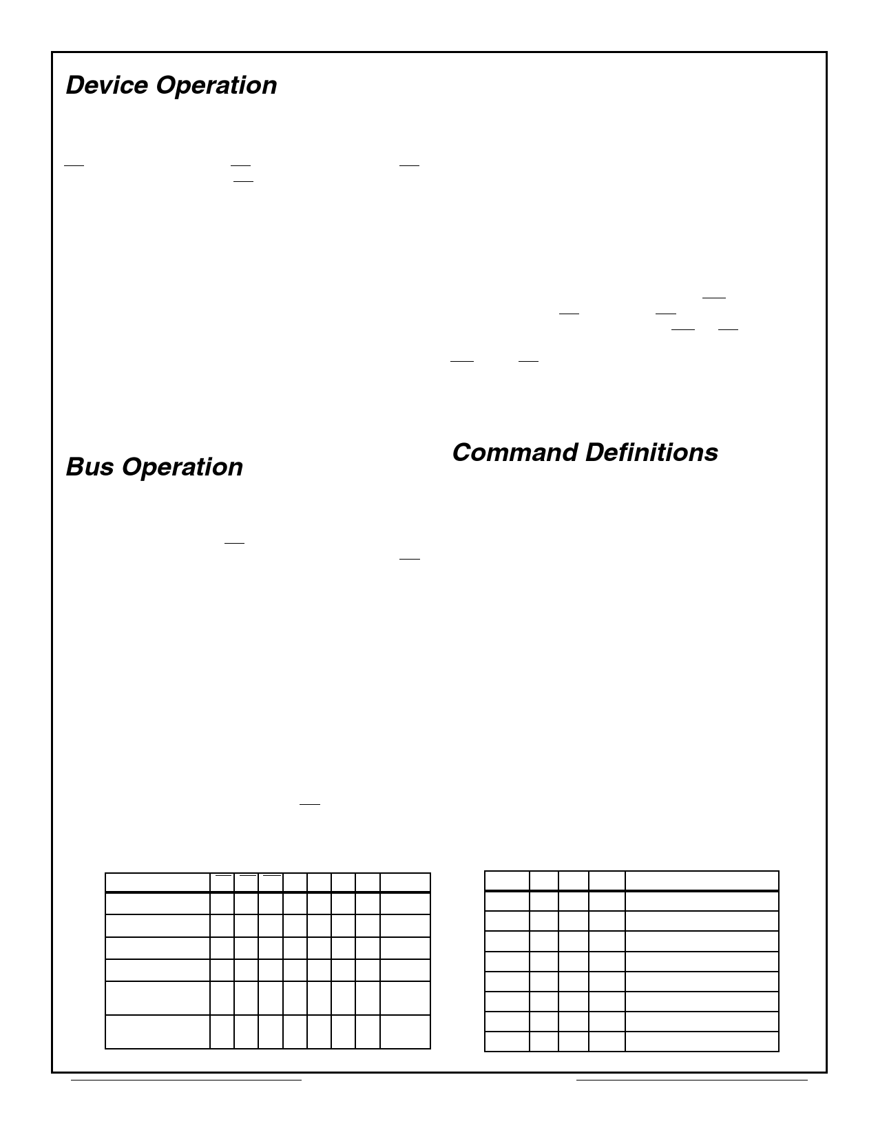
Table 1 – Bus Operations
Operation
CE OE WE A0 A1 A6 A9 I/O
READ
L L H A0 A1 A6 A9 DOUT
STANDBY
H X X X X X X HIGH Z
OUTPUT DISABLE L H H X X X X HIGH Z
WRITE
L H L A0 A1 A6 A9 DIN
ENABLE SECTOR
PROTECT
L VID L
X
X
X VID
X
VERIFY SECTOR
PROTECT
L
L
H
L
H
L VID Code
Table 2 – Sector Addresses Table
A18 A17 A16
SA0 0 0 0
SA1 0 0 1
SA2 0 1 0
SA3 0 1 1
SA4 1 0 0
SA5 1 0 1
SA6 1 1 0
SA7 1 1 1
Address Range
00000h – 0FFFFh
10000h – 1FFFFh
20000h – 2FFFFh
30000h – 3FFFFh
40000h – 4FFFFh
50000h – 5FFFFh
60000h – 6FFFFh
70000h – 7FFFFh
Aeroflex Circuit Technology
5
SCD1665 REV B 6/29/01 Plainview NY (516) 694-6700
Share Link: 