74HC1G00 Просмотр технического описания (PDF) - Philips Electronics
Номер в каталоге
Компоненты Описание
Список матч
74HC1G00 Datasheet PDF : 16 Pages
| |||
Philips Semiconductors
2-input NAND gate
Product specification
74HC1G00; 74HCT1G00
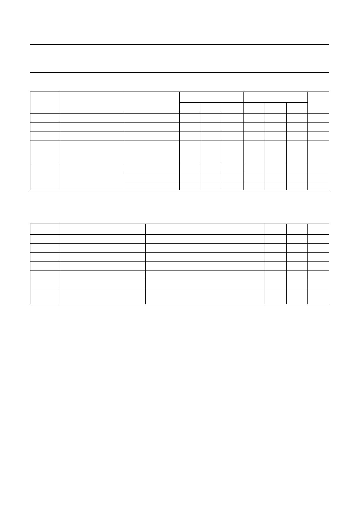
RECOMMENDED OPERATING CONDITIONS
SYMBOL
PARAMETER
CONDITIONS
VCC
VI
VO
Tamb
tr,tf
supply voltage
input voltage
output voltage
operating ambient
temperature
input rise and fall times
see DC and AC
characteristics per
device
VCC = 2.0 V
VCC = 4.5 V
VCC = 6.0 V
74HC1G
74HCT1G
UNIT
MIN. TYP. MAX. MIN. TYP. MAX.
2.0 5.0 6.0 4.5 5.0 5.5 V
0
−
VCC 0
−
VCC V
0
−
VCC 0
−
VCC V
−40 +25 +125 −40 +25 +125 °C
−
−
1000 −
−
−
ns
−
−
500 −
−
500 ns
−
−
400 −
−
−
ns
LIMITING VALUES
In accordance with the Absolute Maximum Rating System (IEC 60134); voltages are referenced to GND (ground = 0 V);
see note 1 and 2.
SYMBOL
PARAMETER
VCC
supply voltage
IIK
input diode current
IOK
output diode current
IO
output source or sink current
ICC
VCC or GND current
Tstg
storage temperature
PD
power dissipation per package
CONDITIONS
VI < −0.5 V or VI > VCC + 0.5 V
VO < −0.5 V or VO > VCC + 0.5 V
−0.5 V < VO < VCC + 0.5 V
for temperature range from −40 to +125 °C;
note 3
MIN.
−0.5
−
−
−
−
−65
−
MAX.
+7.0
±20
±20
±12.5
±25
+150
200
UNIT
V
mA
mA
mA
mA
°C
mW
Notes
1. Stresses beyond those listed may cause permanent damage to the device. These are stress rating only and
functional operation of the device at these or any other conditions beyond those under ‘recommended operating
conditions’ is not implied. Exposure to absolute maximum rated conditions for extended periods may affect device
reliability.
2. The input and output voltage ratings may be exceeded if the input and output current ratings are observed.
3. Above 55 °C the value of PD derates linearly with 2.5 mW/K.
2002 May 15
4
Share Link: 