74HC299(2016) Просмотр технического описания (PDF) - NXP Semiconductors.
Номер в каталоге
Компоненты Описание
Список матч
74HC299 Datasheet PDF : 20 Pages
| |||
Nexperia
74HC299
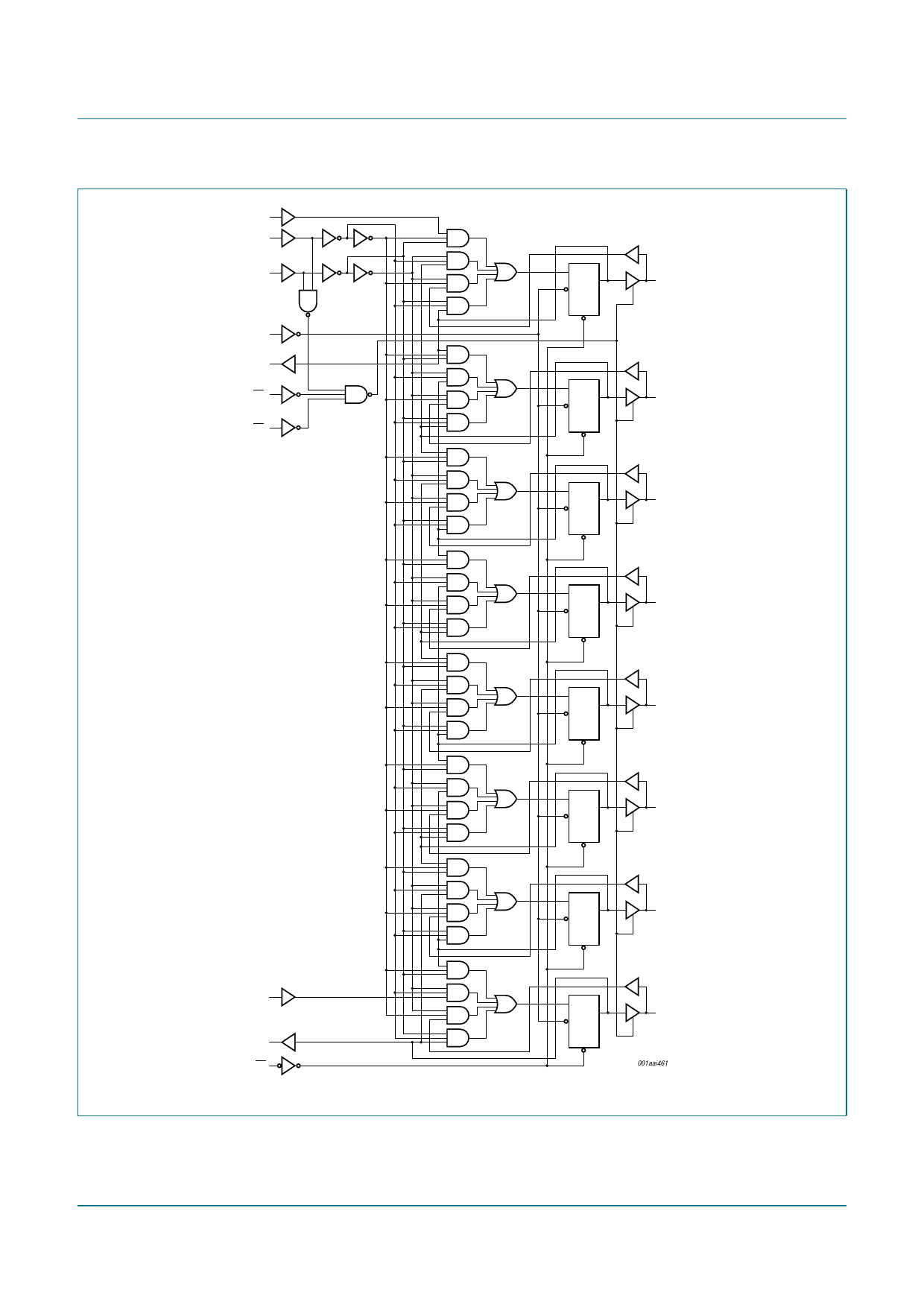
8-bit universal shift register; 3-state
5. Pinning information
5.1 Pinning
+&
6
2(
2(
,2
,2
,2
,2
4
05
*1'
Fig 5. Pin configuration (SO20 and (T)SSOP20)
9&&
6
'6/
4
,2
,2
,2
,2
&3
'65
DDL
5.2 Pin description
Table 2. Pin description
Symbol
Pin
Description
S0, S1
1, 19
mode select input
OE1, OE2
2, 3
3-state output enable input (active LOW)
I/O0, I/O1, I/O2, I/O3, I/O4, I/O5, I/O6, I/O7 7, 13, 6, 14, 5, 15, 4, 16 parallel data input or 3-state parallel output (bus
driver)
Q0, Q7
8, 17
serial output (standard output)
MR
9
asynchronous master reset input (active LOW)
GND
10
ground (0 V)
DSR
11
serial data shift-right input
CP
12
clock input (LOW to HIGH, edge-triggered)
DSL
18
serial data shift-left input
VCC
20
positive supply voltage
74HC299
Product data sheet
All information provided in this document is subject to legal disclaimers.
Rev. 4 — 26 February 2016
© Nexperia B.V. 2017. All rights reserved
4 of 20
Share Link: 