AD8341 Просмотр технического описания (PDF) - Analog Devices
Номер в каталоге
Компоненты Описание
Список матч
AD8341 Datasheet PDF : 20 Pages
| |||
REF LVL
MARKER 1 [T1 ]
–18.47dBm
–12dBm
1.95999900GHz
–12
0.3dB OFFSET
1
–20
–30
RBW 30kHz
VBW 100kHz
SWT 500ms
RF ATT 0dB
UNIT dBm
1 [T1]
–18.47dBm
1.95999900GHz
A
CH PWR
–4.06dBm
ACP UP
–77.64dBm
ACP LOW
–76.66dBm
–40
1AVG
–50
1RM
–60
–70
–80
–90
–100
C11
C11
C0
C0
CU1 CU1
–112
CENTER 1.96Hz
1MHz/
SPAN 10MHz
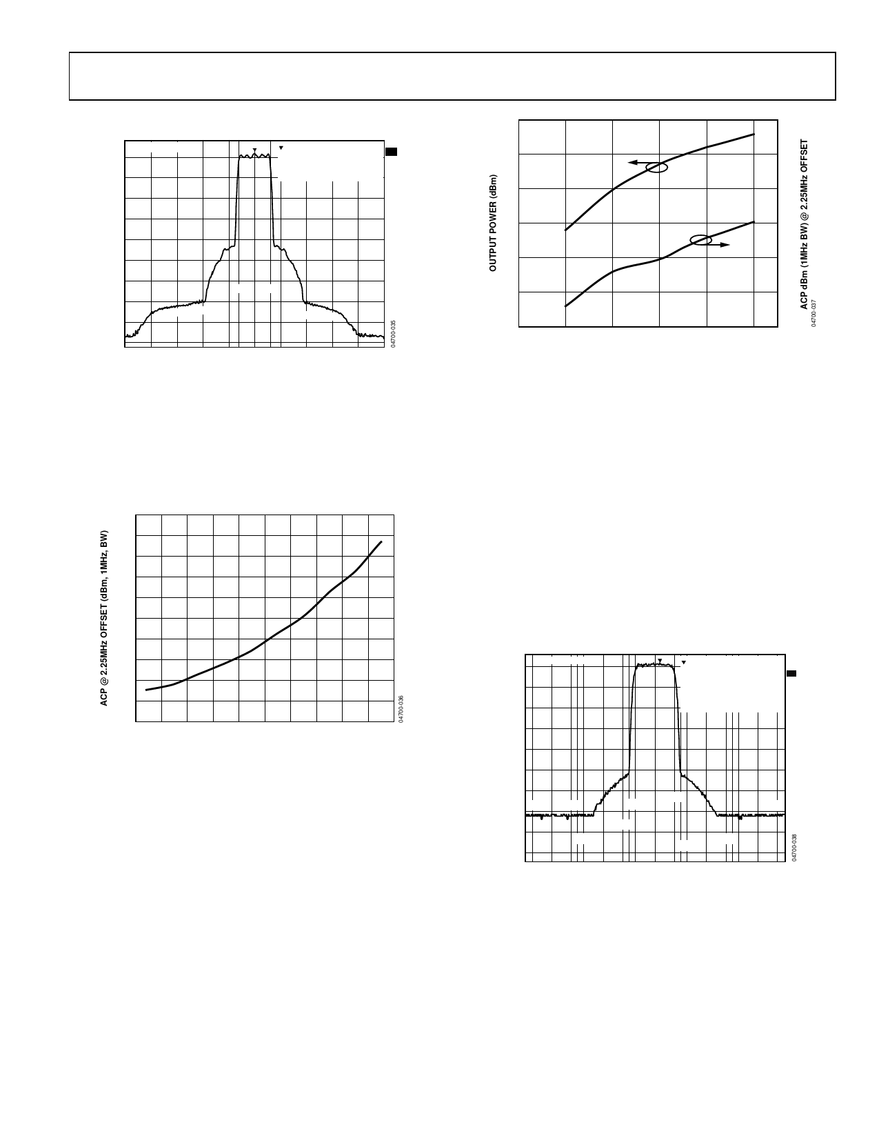
Figure 35. Output Spectrum, 1960 MHz, Single-Carrier CDMA2000
Test Model at −4 dBm, VBBI = VBBQ = 0.353 V, Adjacent Channel Power
Measured at ±2.25 MHz Carrier Offset in 1 MHz BW Input Signal Filtered
Using a Cavity Tuned Filter (Pass Band = 6.8 MHz)
Holding the differential I and Q control voltages steady at
0.353 V, input power was swept. Figure 36 shows variation in
spurious content, again measured at ±2.25 MHz carrier offset in
a 1 MHz bandwidth, as defined by the 3GPP2 specification.
–70
–72
–74
–76
–78
–80
–82
–84
–86
–88
–90
–20 –18 –16 –14 –12 –10 –8 –6 –4 –2 0
OUTPUT POWER (dBm)
Figure 36. Adjacent Channel Power vs. Output Power,
CDMA2000 Single Carrier @ 1960 MHz; ACP Measured at
±2.25 MHz Carrier Offset (1 MHz BW); VBBI = VBBQ = 0.353 V
With a fixed input power of 2.4 dBm, the output power was
again swept by exercising the I and Q inputs. VBBI and VBBQ were
kept equal and were swept from 100 mV to 500 mV. The result-
ing output power and ACP are shown in Figure 37.
AD8341
0
–60
–5
–65
–10
–70
–15
–75
–20
–80
–25
–85
–30
0
0.1
0.2
0.3
0.4
IQ CONTROL VOLTAGE
–90
0.5
Figure 37. Output Power and ACP vs. I and Q Control Voltages,
CDMA2000 Test Model, VBBI = VBBQ, ACP Measured at
±2.25 MHz Carrier Offset in 1 MHz BW
Figure 37 shows that for a fixed input power, the ACP (measured in
dBm) tracks the output power as the gain is changed.
WCDMA APPLICATION
Figure 38 shows a plot of the output spectrum of the AD8341
transmitting a single-carrier WCDMA signal (Test Model 1-64
at 2140 MHz). The carrier power is approximately −9 dBm. The
differential I and Q control voltages are both equal to 0.353 V,
that is, the vector is sitting on the unit circle at 45°. At this
power level, an adjacent channel power ratio of −61 dBc is
achieved. The alternate channel power ratio of −72 dBc is
dominated by the noise floor of the AD8341.
REF LVL
MARKER 1 [T1 ]
–28.39dBm
–24 –24dBm
2.14050000GHz
OFFSET 1dB
–30
–40
–50
–60
RBW 30kHz
RF ATT 0dB
VBW 300kHz
SWT 1s
UNIT dBm
1
1 [T1]
–28.39dBm
CH PWR
2.14050000GHz
–8.95dBm
A
ACP UP
–60.78dB
ACP LOW
–60.82dB
ALT1 UP
–72.67dB
ALT1 LOW
–72.66dB
1RM
–70
–80
–90
C12
C12
–100
–110
C11
–120
–124
CENTER 2.14GHz
C0
C0
C11
CU1
2.5MHz/
CU2
CU1
SPAN 25MHz
Figure 38. AD8341 Single-Carrier WCDMA Spectrum at 2140 MHz
Figure 39 shows how ACPR and noise vary with varying input
power (differential I and Q control voltages are held at 0.353 V).
At high power levels, both adjacent and alternate channel power
ratios increase sharply. As output power drops, adjacent and
alternate channel power ratios both reach minimums before the
measurement becomes dominated by the noise floor of the
AD8341. At this point, adjacent and alternate channel power
ratios become approximately equal.
Rev. 0 | Page 15 of 20
Share Link: 