UPD72850A Просмотр технического описания (PDF) - NEC => Renesas Technology
Номер в каталоге
Компоненты Описание
Список матч
UPD72850A Datasheet PDF : 48 Pages
| |||
3. INTERNAL FUNCTION
3.1 Link Interface
3.1.1 Connection Method
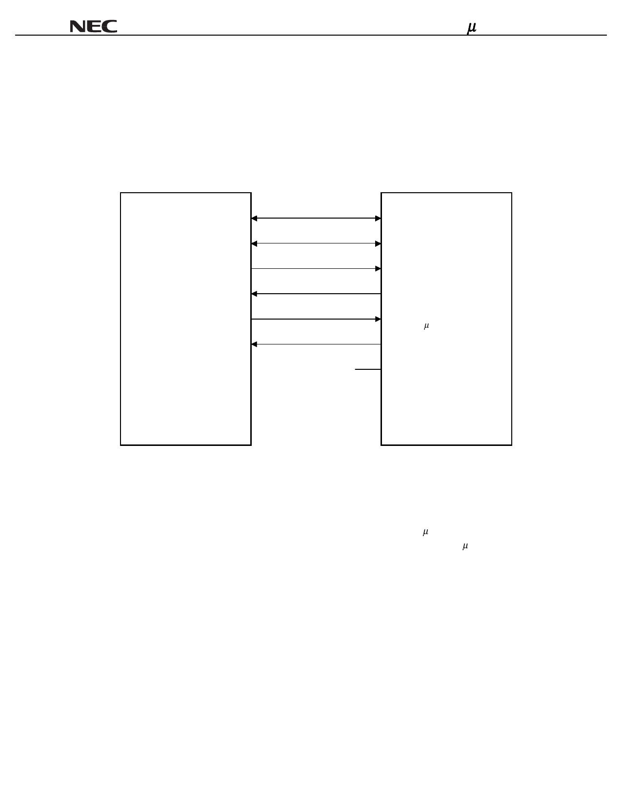
Figure 3-1. PHY/Link Connection Method
µPD72850A
D0-D7
CTL0,CTL1
LREQ
SCLK
LPS
PHY
Link
µP D 7 2 8 5 0 A
LKON
Note
DIRECT
Note Clamping to VDD provides direct connection to Link.
Clamping to GND connects through isolation barrier to Link.
The isolation barrier connection circuit is described in 3.1.7 Isolation Barrier.
3.1.2 LPS (Link Power Status)
LPS is a function to monitor the On/Off status of the Link power supply. After 1.2 µsec or more, LPS is Low, the
PHY/Link is reset and D and CTL are output Low (when the isolation barrier is Hi-Z). After 2.5 µsec or more, LPS is
Low, moreover, the PHY stops the supply of SCLK and SCLK outputs Low (when the isolation barrier is Hi-Z).
3.1.3 LREQ, CTL0,CTL1, and D0-D7 Pins
LREQ
: Indicates that a request is received from Link.
CTL0,CTL1 : Bi-directional pin which controls the functions between the PHY/Link interface.
D0-D7
: Bi-directional pin which controls the data Transfer/Receive status signal, and the speed code
Transfer/Receive status signal.
3.1.4 SCLK
49.152 MHz clock supplied by PHY for the PHY/Link interface synchronization.
Data Sheet S14452EJ1V0DS00
15
Share Link: 