W83193R-01 Просмотр технического описания (PDF) - Winbond
Номер в каталоге
Компоненты Описание
Список матч
W83193R-01 Datasheet PDF : 19 Pages
| |||
W83193R-01
7.0 FUNTION DESCRIPTION
7.1 POWER MANAGEMENT FUNCTIONS
PRELIMINARY
All clocks can be individually enabled or disabled via the 2-wire control interface. On power up,
external circuitry should allow 3 ms for the VCO’s to stabilize prior to enabling clock outputs to
assure correct pulse widths. When MODE=0, pins 15 and 46 are inputs (PCI_STOP#),
(CPU_STOP#), when MODE=1, these functions are not available. A particular clock could be
enabled as both the 2-wire serial control interface and one of these pins indicate that it should be
enable.
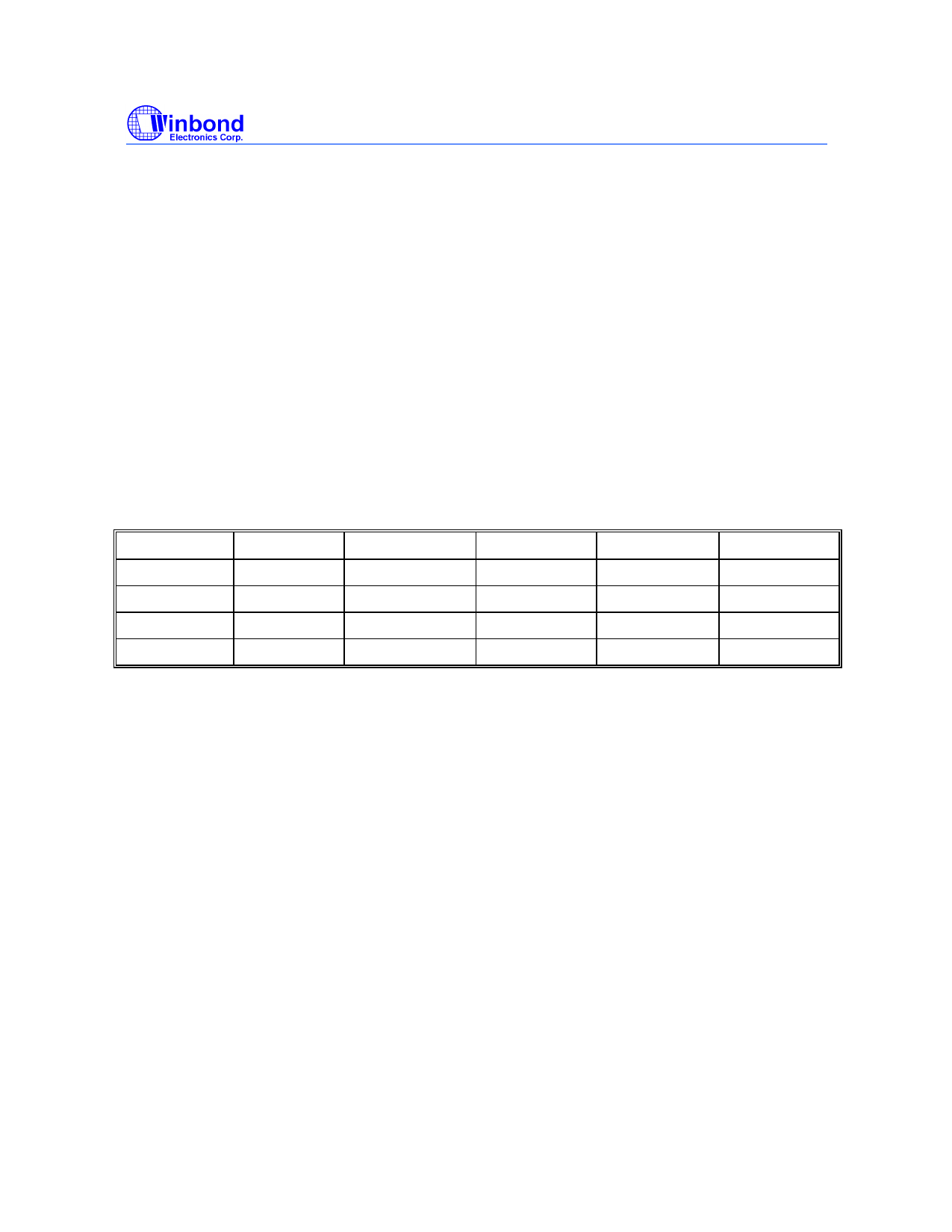
The W83193R-01 may be disabled in the low state according to the following table in order to reduce
power consumption. All clocks are stopped in the low state, but maintain a valid high period on
transitions from running to stop. The CPU and PCI clocks transform between running and stop by
waiting for one positive edge on PCICLK_F followed by negative edge on the clock of interest, after
which high levels of the output are either enabled or disabled.
CPU_STOP#
0
0
1
1
PCI_STOP#
0
1
0
1
CPU
LOW
LOW
RUNNING
RUNNING
PCI
LOW
RUNNING
LOW
RUNNING
OTHER CLKs
RUNNING
RUNNING
RUNNING
RUNNING
XTAL & VCOs
RUNNING
RUNNING
RUNNING
RUNNING
7.2 2-WIRE I2C CONTROL INTERFACE
The 2-wire control interface implements a write only slave interface and cannot be read back. All
proceeding bytes must be sent to change one of the control bytes. The 2-wire control interface allows
each clock output individually enabled or disabled. On power up, the W83193R-01 initializes with
default register settings, and then it’s optional to use the 2-wire control interface.
The SDATA signal only changes when the SDCLK signal is low, and is stable when SDCLK is high
during normal data transfer. There are only two exceptions. One is a high-to-low transition on
SDATA while SDCLK is high used to indicate the beginning of a data transfer cycle. The other is a
low-to-high transition on SDATA while SDCLK is high used to indicate the end of a data transfer
cycle. Data is always sent as complete 8-bit bytes followed by an acknowledge generated.
Byte writing starts with a “start” condition followed by 7-bit slave address and a write command bit
[1101 0010], command code checking [0000 0000], and byte count checking. After successful
reception of each byte, an “acknowledge“ (low) on the SDATA wire will be generated by the clock
chip. Controller can start to write to internal I2C registers after the string of data. The sequence
order is as follows:
Publication Release Date: May 1998
-6-
Revision 0.20
Share Link: 