W83193R-01 Просмотр технического описания (PDF) - Winbond
Номер в каталоге
Компоненты Описание
Список матч
W83193R-01 Datasheet PDF : 19 Pages
| |||
W83193R-01
8.0 SPECIFICATIONS
PRELIMINARY
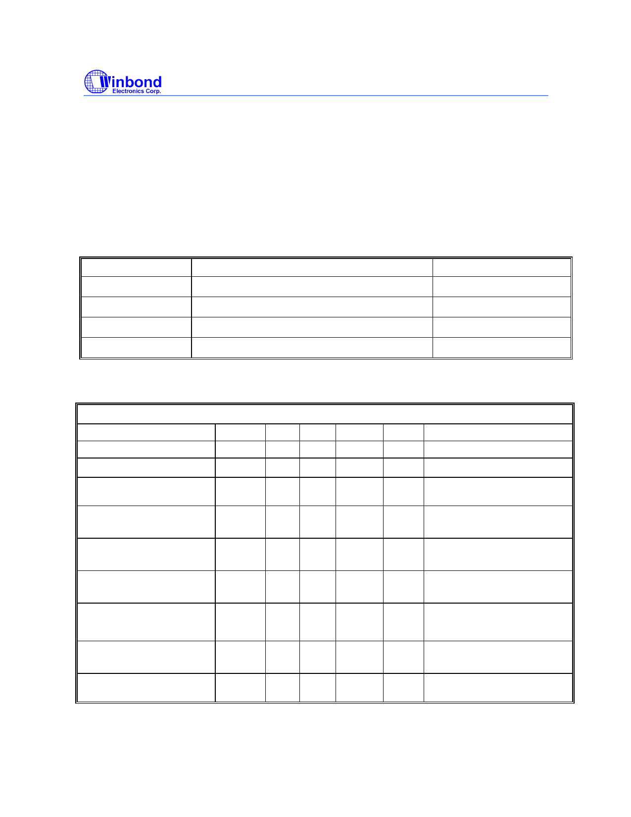
8.1 ABSOLUTE MAXIMUM RATINGS
Stresses greater than those listed in this table may cause permanent damage to the device.
Precautions should be taken to avoid application of any voltage higher than the maximum rated
voltages to this circuit. Maximum conditions for extended periods may affect reliability. Unused
inputs must always be tied to an appropriate logic voltage level (Ground or Vdd).
Symbol
Vdd , VIN
TSTG
TB
TA
Parameter
Voltage on any pin with respect to GND
Storage Temperature
Ambient Temperature
Operating Temperature
Rating
- 0.5 V to + 7.0 V
- 65°C to + 150°C
- 55°C to + 125°C
0°C to + 70°C
8.2 AC CHARACTERISTICS
Vdd = Vddq3 = 3.3V ± 5 %, Vddq2= 2.375V~2.9V , TA = 0°C to +70°C
Parameter
Symbol Min Typ Max Units
Output Duty Cycle
45 50
55
%
CPU/SDRAM to PCI Offset
tOFF
1
4
ns
Skew (CPU-CPU), (PCI-
PCI), (SDRAM-SDRAM)
CPU/SDRAM
Cycle to Cycle Jitter
tSKEW
tCCJ
250
ps
¡Ó250 ps
CPU/SDRAM
tJA
Absolute Jitter
500
ps
Jitter Spectrum 20 dB
BWJ
500 KHz
Bandwidth from Center
Output Rise (0.4V ~ 2.0V)
& Fall (2.0V ~0.4V) Time
tTLH
0.4
tTHL
1.6
ns
Overshoot/Undershoot
Vover
0.7
1.5
V
Beyond Power Rails
Ring Back Exclusion
VRBE
0.7
2.1
V
Test Conditions
Measured at 1.5V
15 pF Load Measured at 1.5V
15 pF Load Measured at 1.5V
15 pF Load on CPU and PCI
outputs
22 Ω at source of 8 inch PCB
run to 15 pF load
Ring Back must not enter this
range.
- 10 -
Publication Release Date: May 1998
Revision 0.20
Share Link: 