HS-80C86RH Просмотр технического описания (PDF) - Intersil
Номер в каталоге
Компоненты Описание
Список матч
HS-80C86RH Datasheet PDF : 29 Pages
| |||
HS-80C86RH
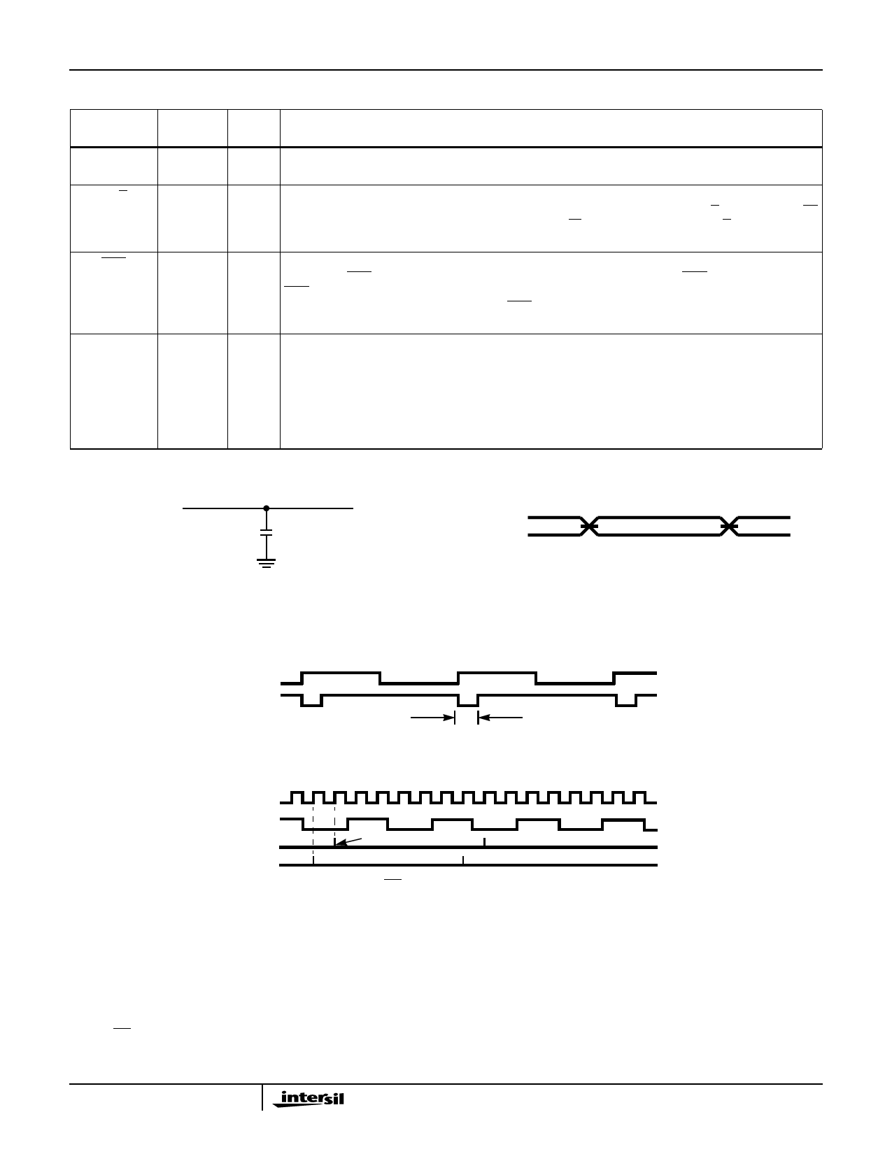
Pin Descriptions (Continued)
SYMBOL
PIN
NUMBER TYPE
DESCRIPTION
ALE
25
O ADDRESS LATCH ENABLE: is provided by the processor to latch the address into the 82C82 latch. It is
a HIGH pulse active during clock LOW of T1 of any bus cycle. Note that ALE is never floated.
DT/R
27
O DATA TRANSMIT/RECEIVE: is needed in a minimum system that desires to use a data bus transceiver.
It is used to control the direction of data flow through the transceiver. Logically, DT/R is equivalent to S1
in maximum mode, and its timing is the same as for M/IO (T = HlGH, R = LOW). DT/R is held to a high
impedance logic one during local bus “hold acknowledge”.
DEN
26
O DATA ENABLE: provided as an output enable for a bus transceiver in a minimum system which uses the
transceiver. DEN is active LOW during each memory and I/O access and for INTA cycles. For a read or
INTA cycle it is active from the middle of T2 until the middle of T4, while for a write cycle it is active from
the beginning of T2 until the middle of T4. DEN is held to a high impedance logic one during local bus
“hold acknowledge”.
HOLD
HLDA
31
I HOLD: indicates that another master is requesting a local bus “hold”. To be a acknowledged, HOLD must
30
O be active HIGH. The processor receiving the “hold” will issue a “hold acknowledge” (HLDA) in the middle
of a T4 or T1 clock cycle. Simultaneously with the issuance of HLDA, the processor will float the local bus
and control lines. After HOLD is detected as being LOW, the processor will lower HLDA, and when the
processor needs to run another cycle, it will again drive the local bus and control lines.
HOLD is not an asynchronous input. External synchronization should be provided if the system cannot
otherwise guarantee the setup time.
AC Test Circuit
OUTPUT FROM
DEVICE UNDER TEST
CL (NOTE)
TEST POINT
NOTE: Includes stray and jig capacitance.
AC Testing Input, Output Waveform
INPUT
VIH
VIL - 0.4V
1.5V
1.5V
OUTPUT
VOH
VOH
NOTE: All inputs signals (other than CLK) must switch between VIL
Max -0.4V and VIH Min +0.4. CLK must switch between 0.4V and
VDD -0.4V. TR and TF must be less than or equal to 15ns. CLK TR
and TF must be less than or equal to 10ns.
Timing Diagrams
F5
READY
4T
READY TIMING AS COMPARED TO F5
F14
F16
RESET
PULSE
NMI
RESET, NMI, AND MN/MX TIMING AS COMPARED TO F14 AND F16
NOTES:
4. F0 = 100kHz, 50% duty cycle square wave.
F1 = F0/2, F2 = F1/2 . . . F16 = F15/2.
5. READY, RESET, and NMI timing are as shown: T = 10µs.
6. All signals have rise/fall time limits: 100ns < t-rise, t-fall < 500ns.
7. RESET has a pulse width = 8T and occurs every two cycles of F16.
8. NMI has a pulse width = 4T and occurs every two cycles of F16.
9. MN/MX is a 50% duty cycle square wave and changes every eight cycles of F16.
7
Share Link: 