HS-80C86RH Просмотр технического описания (PDF) - Intersil
Номер в каталоге
Компоненты Описание
Список матч
HS-80C86RH Datasheet PDF : 29 Pages
| |||
HS-80C86RH
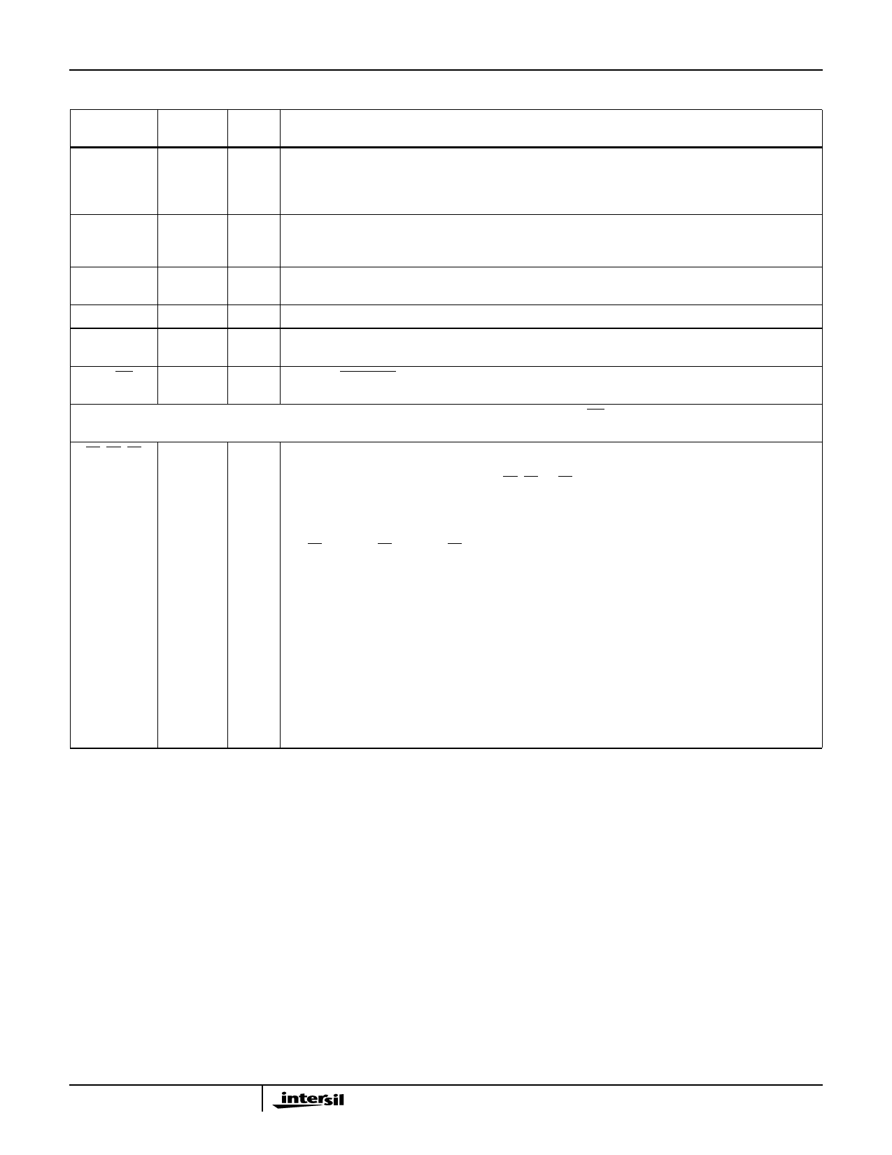
Pin Descriptions (Continued)
SYMBOL
PIN
NUMBER TYPE
DESCRIPTION
NMI
17
I NON-MASKABLE INTERRUPT: is an edge triggered input which causes a type 2 interrupt. An interrupt
service routine is called via an interrupt vector lookup table located in system memory. NMI is not
maskable internally by software. A transition from LOW to HIGH initiates the interrupt at the end of the
current instruction. This input is internally synchronized.
RESET
21
I RESET: causes the processor to immediately terminate its present activity. The signal must change from
LOW to HIGH and remain active HIGH for at least 4 CLK cycles. It restarts execution, as described in the
Instruction Set description, when RESET returns LOW. RESET is internally synchronized.
CLK
19
I CLOCK: provides the basic timing for the processor and bus controller. It is asymmetric with a 33% duty
cycle to provide optimized internal timing.
VDD
40
VDD: +5V power supply pin. A 0.1µF capacitor between pins 20 and 40 is recommended for decoupling.
GND
1, 20
GND: Ground. Note: both must be connected. A 0.1µF capacitor between pins 1 and 20 is
recommended for decoupling.
MN/MX
33
I MINIMUM/MAXIMUM: Indicates what mode the processor is to operate in. The two modes are discussed
in the following sections.
The following pin function descriptions are for the HS-80C86RH system in maximum mode (i.e., MN/MX = GND). Only the pin functions which are
unique to maximum mode are described below.
S0, S1, S2
26-28
O STATUS: is active during T4, T1 and T2 and is returned to the passive state (1,1,1) during T3 or during
TW when READY is HIGH. This status is used by the 82C88 Bus Controller to generate all memory and
I/O access control signals. Any change by S2, S1, or S0 during T4 is used to indicate the beginning of a
bus cycle, and the return to the passive state in T3 or TW is used to indicate the end of a bus cycle. These
status lines are encoded. These signals are held at a high impedance logic one state during “grant
sequence”.
S2
S1
S0
0
0
0
Interrupt Acknowledge
0
0
1
Read I/O Port
0
1
0
Write I/O Port
0
1
1
Halt
1
0
0
Code Access
1
0
1
Read Memory
1
1
0
Write Memory
1
1
1
Passive
5
Share Link: 