CS61881-IB Просмотр технического описания (PDF) - Cirrus Logic
Номер в каталоге
Компоненты Описание
Список матч
CS61881-IB Datasheet PDF : 28 Pages
| |||
CS61881
2. THEORY OF OPERATION
The CS61881 is designed to provide the analog
front end (AFE) for up to eight E1 lines. The device
provides an interface to twisted pair or co-axial me-
dia. A patented matched impedance technique is
employed that reduces power and eliminates the
need for matching resistors. As a result, the device
can interface directly to the line through a trans-
former without the need for matching resistors on
either the receive side or the transmit side.
2.1 Transmitter
The CS61881 contains eight identical transmitters
that each use a low power matched impedance driv-
er to eliminate the need for external load matching
resistors. As a result, the TTIP/TRING outputs can
be direct connected to the pulse transformer allow-
ing one hardware circuit for both 120 Ω and 75 Ω
applications (see the Applications section). In addi-
tion, the matched impedance driver provides im-
proved return loss when compared to solutions
with external matching resistors. The appropriate
line matching is selected via the CBLSEL control
pin.
The line drivers transmit data received in either
NRZ or RZ format depending on the state of
TCLK. When TCLK is driven with an external
clock, NRZ data sampled on TPOS/TNEG will be
transmitted onto the line via TTIP/TRING. In this
mode, a transmit pulse shape compliant to G.703
will be generated internally (see Figure 4). Data on
TPOS/TNEG is sampled on the falling edge of
TCLK.
If TCLK is held high for at least 12 µS, RZ data
driven into TPOS/TNEG is transmitted on
TTIP/TRING. In this mode, the width of positive
pulses is controlled by the width of the pulses on
TPOS and the width of negative pulses is con-
trolled by the width of the pulses on TNEG.
The transmitter can be forced into a high impedance,
low power state by holding TCLK low. Alternately,
the TXOE pin can be used to force all eight trans-
mitters into a high impedance state. This feature is
useful in applications that require redundancy.
Percent of
nominal
peak
voltage
120
110
100
90
80
269 ns
244 ns
194 ns
50
10
Nominal Pulse
0
-10
-20
219 ns
488 ns
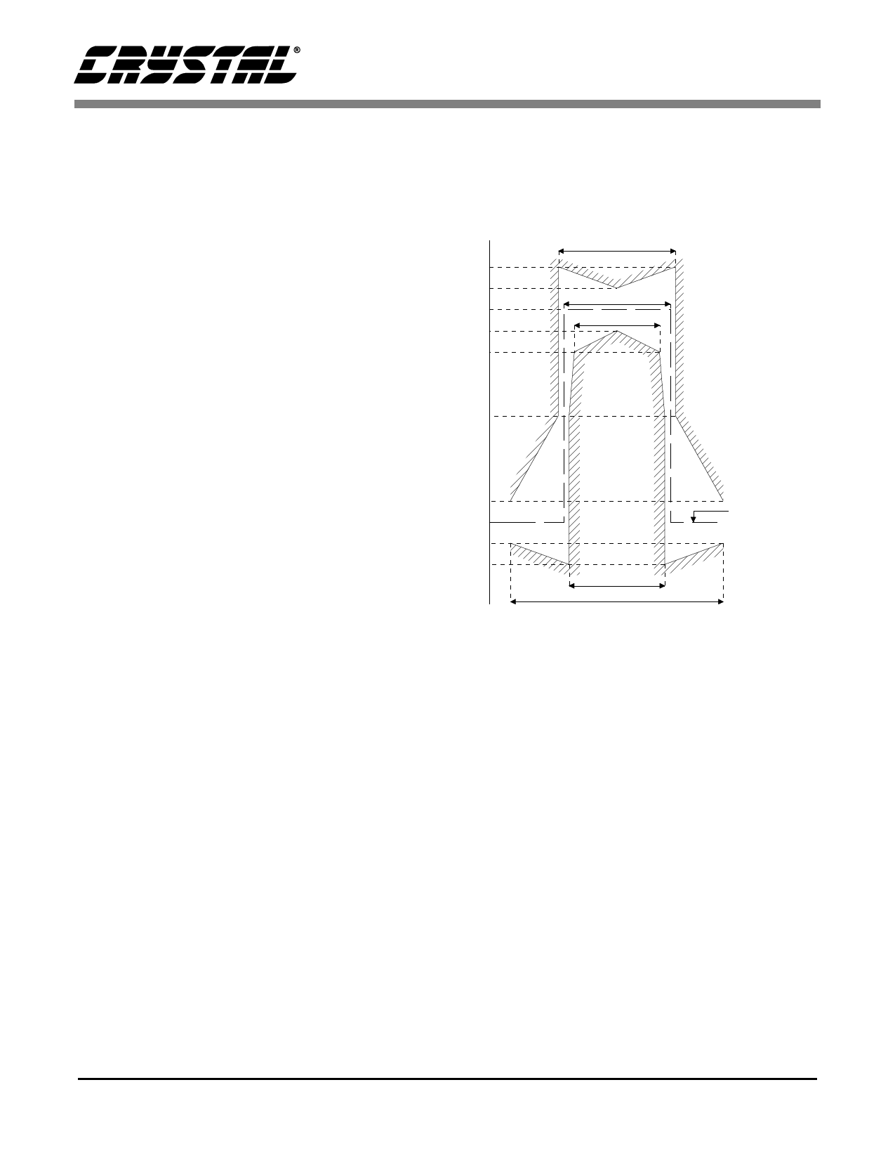
Figure 4. Mask of the Pulse at the 2048 kbps Interface
2.2 Receiver
The CS61881 contains eight identical receivers that
each use a matched impedance technique that al-
lows a common set of external components for both
120 Ω and 75 Ω operation. This allows one stuffing
option to accommodate both line impedances. The
appropriate line matching is set via the CBLSEL
pin.
The receiver slices the incoming signal on
RTIP/RING and outputs the recovered data on
RPOS/RNEG. To maximize the signal-to-noise ra-
tio, the slicing threshold is dynamically adjusted
based on the amplitude of the incoming signal. In
the absence of a signal, a minimum threshold is
maintained to reduce the occurrence of impulse
noise. The receiver is capable of recovering signals
with over 12 dB of attenuation (referenced to
2.37 V nominal).
DS451PP3
9
Share Link: 