STD6NF10 Просмотр технического описания (PDF) - STMicroelectronics
Номер в каталоге
Компоненты Описание
Список матч
STD6NF10
STMicroelectronics

STD6NF10 Datasheet PDF : 14 Pages
| |||
Electrical characteristics
2
Electrical characteristics
STD6NF10, STU6NF10
(TCASE = 25 °C unless otherwise specified)
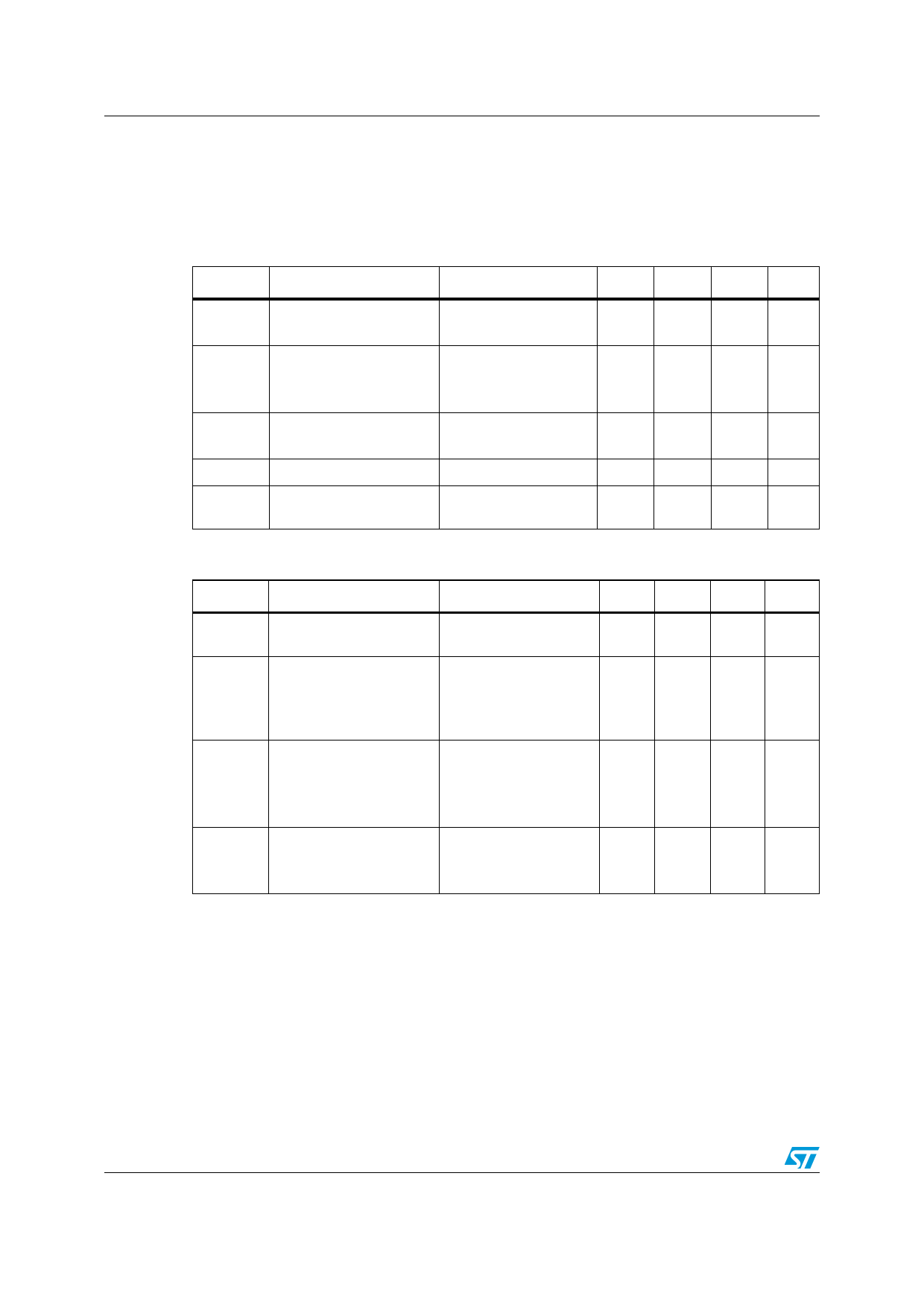
Table 4. On/off states
Symbol
Parameter
Drain-source
V(BR)DSS breakdown voltage
IDSS
Zero gate voltage
drain current (VGS = 0)
IGSS
VGS(th)
RDS(on)
Gate-body leakage
current (VDS = 0)
Gate threshold voltage
Static drain-source on
resistance
Test conditions
Min.
ID = 250 µA, VGS =0
100
VDS = max rating
VDS =max rating,
TC = 125 °C
VGS = ± 20 V
VDS = VGS, ID = 250 µA
2
VGS = 10 V, ID = 3 A
Typ. Max. Unit
V
1
µA
10
µA
±100 nA
4
V
0.22 0.25
Ω
Table 5.
Symbol
Dynamic
Parameter
Test conditions
Min.
gfs (1)
Ciss
Coss
Crss
Forward
transconductance
Input capacitance
Output capacitance
Reverse transfer
capacitance
VDS = > ID(on) x
RDS(on)max, ID = 3A
VDS = 25 V, f = 1 MHz,
VGS = 0
td(on)
tr
td(off)
tf
Turn-on delay time
Rise time
Turn-off delay time
Fall time
VDD = 50 V, ID = 3 A
RG = 4.7 Ω, VGS = 10 V
(see Figure 13)
Qg
Total gate charge
Qgs Gate-source charge
Qgd Gate-drain charge
VDD = 80 V, ID = 6 A,
VGS = 10 V, RG = 4.7 Ω
(see Figure 14)
1. Pulsed: Pulse duration = 300 µs, duty cycle 1.5%.
Typ.
34
280
45
20
6
10
20
3
10
2.5
4
Max.
14
Unit
S
pF
pF
pF
ns
ns
ns
ns
nC
nC
nC
4/14
Share Link: