RT9237 Просмотр технического описания (PDF) - Richtek Technology
Номер в каталоге
Компоненты Описание
Список матч
RT9237 Datasheet PDF : 15 Pages
| |||
Preliminary
RT9237
The
sensing
circuit
gets
IX
=
IL × RS
RSP
by
local
feedback.
RSP = RSN to cancel the voltage drop caused by GM
amplifier input bias current. IX is sampled and held
just before low side MOSFET turns off (See Fig.2).
Therefore,
IX(S / H)
=
IL(S / H) × RS
RSP
,
IL(S / H)
=
IL( AVG)
−
VO
L
×
TOFF
2
,
TOFF
=
VIN − VO
VIN
×
5µS
,
for
operating
frequency
=
200kHz
IX(S / H)
=
IL( AVG)
−
VO
−
VIN − VO
VIN
2L
×
5µS
×
RS
RSP
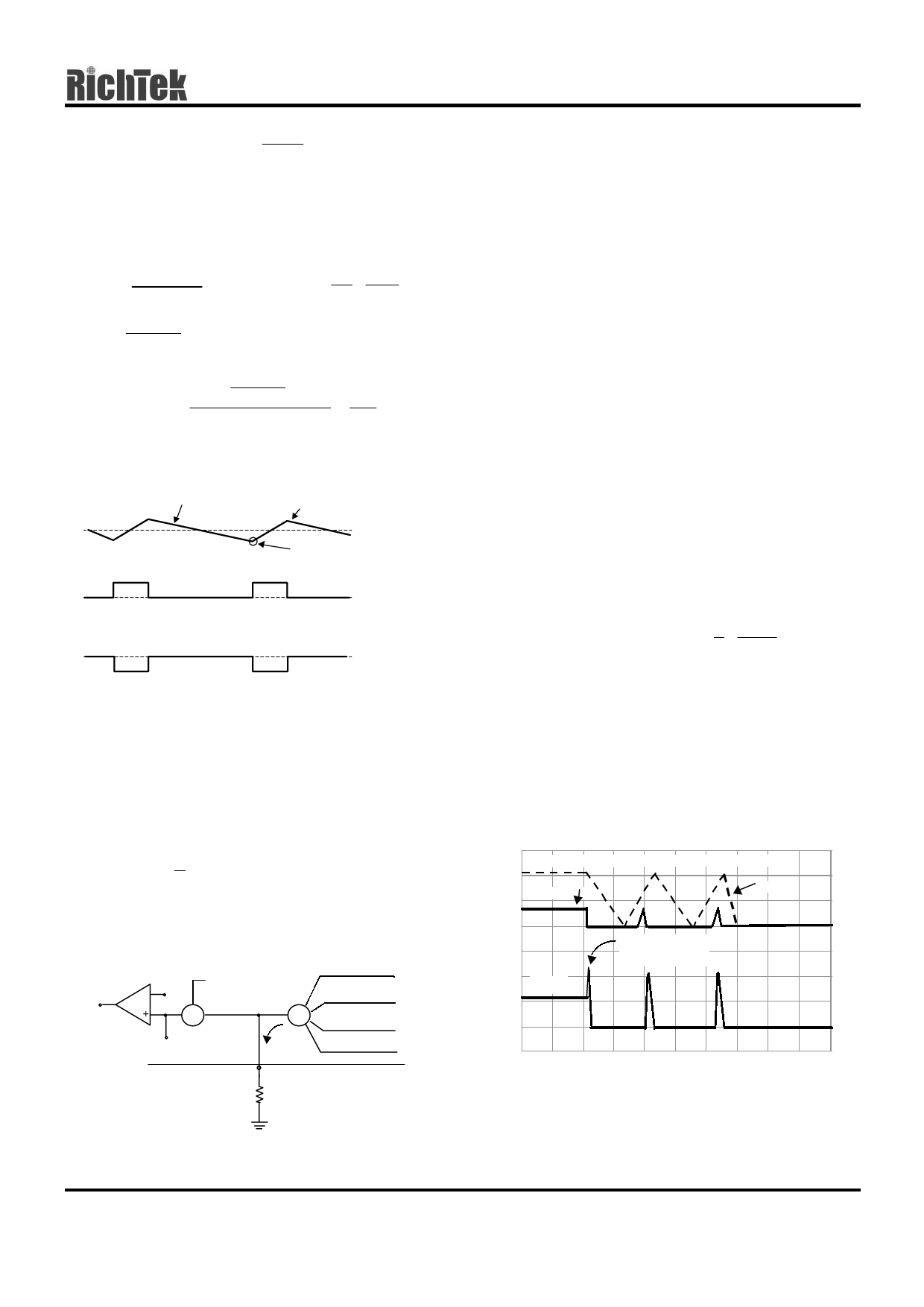
Falling Slope = VO /L IL
Inductor Current
IL (S/H)
IL (AVG)
PWM Signal & High Side MOSFET Gate Signal
Low Side MOSFET Gate Signal
Fig. 2 Inductor Current and PWM Signal
Droop Tuning
The S/H current signals from power channels are
injected to ADJ pin to create droop voltage.
VADJ
=
RADJ
×
2
3
∑ IX
The DAC output voltage decreases by VADJ to form
the VCORE load droop(see Fig.3).
COMP
_
EA
VDAC
FB + _ VADJ
∑
VDAC - VADJ
∑ IX
ADJ
R AD J
2/3 IX1
2/3 IX2
2/3 IX3
2/3 IX4
Protection and SS function
For OVP, the RT9237 detects the VCORE by VSEN
pin. Eliminate the parasitic delay and noise influence
on the PCB path for fast and accurate detection. The
trip point of OVP is 120% of normal output level. The
PWM outputs are pulled low to turn on the low side
MOSFET and turn off the high side MOSFET of the
synchronous rectifier at OVP. The OVP latch can
only be reset by VDD or DVD restart power on reset
sequence. The PGOOD detection trip point of VCORE
is ±8% out of the normal level. The PGOOD open
drain output pulls low when VOCRE exceeds the
range.
Soft start circuit generates a ramp voltage by
charging external capacitor with 10uA current after IC
POR acts. The PWM pulse width and VCORE are
clamped by the rising ramp to reduce the in-rush
current and protect the power devices.
Over current protection trip point is set by the resistor
RchIManAXnecloSnn/HeccteudrretontIMsAigXnaplinIX. >OC32P×
is triggered if one
0.6
RIMAX
.
Controller
forces PWM output latched at high impedance to turn
off both high and low side MOSFET in the power
stage and initial the hiccup mode protection. The SS
pin voltage is pulled low with a 10µA current after it is
less than 90% VDD. The converter restarts after SS
pin voltage < 0.2V. Three times of OCP disable the
converter and only release the latch by POR acts
(see Fig.4).
COUNT = 1 COUNT = 2 COUNT = 3
4V
2V VCORE
SS
0V
IL
OVERLOAD
APPLIED
0A
T0T1
T2
T3T4
TIME
Fig. 4
Fig. 3 Droop Tune Circuit
DS9237-00 January 2002
www.richtek-ic.com.tw
9
Share Link: 