RT9237 Просмотр технического описания (PDF) - Richtek Technology
Номер в каталоге
Компоненты Описание
Список матч
RT9237 Datasheet PDF : 15 Pages
| |||
Preliminary
RT9237
Design Example
Three phase converter VCORE = 1.5V, VIN = 12V, full
load current = 60Amp, droop voltage at full load =
120mV, OCP trip point for each power stage =
30Amp (at Sample/Hold), low side MOSFET RDS(ON)
= 6mΩ at room temperature, L = 2µH, COUT =
9000µF, capacitor ESR = 2m Ω.
1. Compensation setting
a. Modulator Gain, Pole and Zero
Modulator Gain =
VIN
VRAMP
, saw-tooth wave
amplitude
VRAMP
=
1V
×
56kΩ
RIMP
, choose RIRMP
= 39K, VRAMP = 1.4V, modulator Gain = 8.6 =
1
18.7dB, LC
ESR zero =
filter pole
1
2
πCRESR
=
=
2π LC
8.8kHz
= 1.2kHz
,
b. EA compensation network
Use type 2 compensation scheme (see Fig. 5),
,FZ
=
1
2πR2C1
,
mid-band gain
FP =
=
R2
R1
1
2πR2(
C1
C1
×
+
. Choose
C2
C2
R1
)
=
2.4KΩ,
R2
=
24KΩ, C1 = 6.6nF, C2 = 33pF, get FZ = 1KHz,
Fp = 200KHz, mid-band Gain=10=20dB,
modulator asymptotic Bode plot of EA
compensation and PWM loop Gain Bode
shown as Fig. 6.
C1
R2
C2
COMP
_
EA
FB
DACOUT
C3
R3
R1
VCORE
R3, C3 are used in type 3
compensation scheme (left
NC in type 2)
ROL
ROL for no load offset
setting
Fig. 5 EA Compensation Network
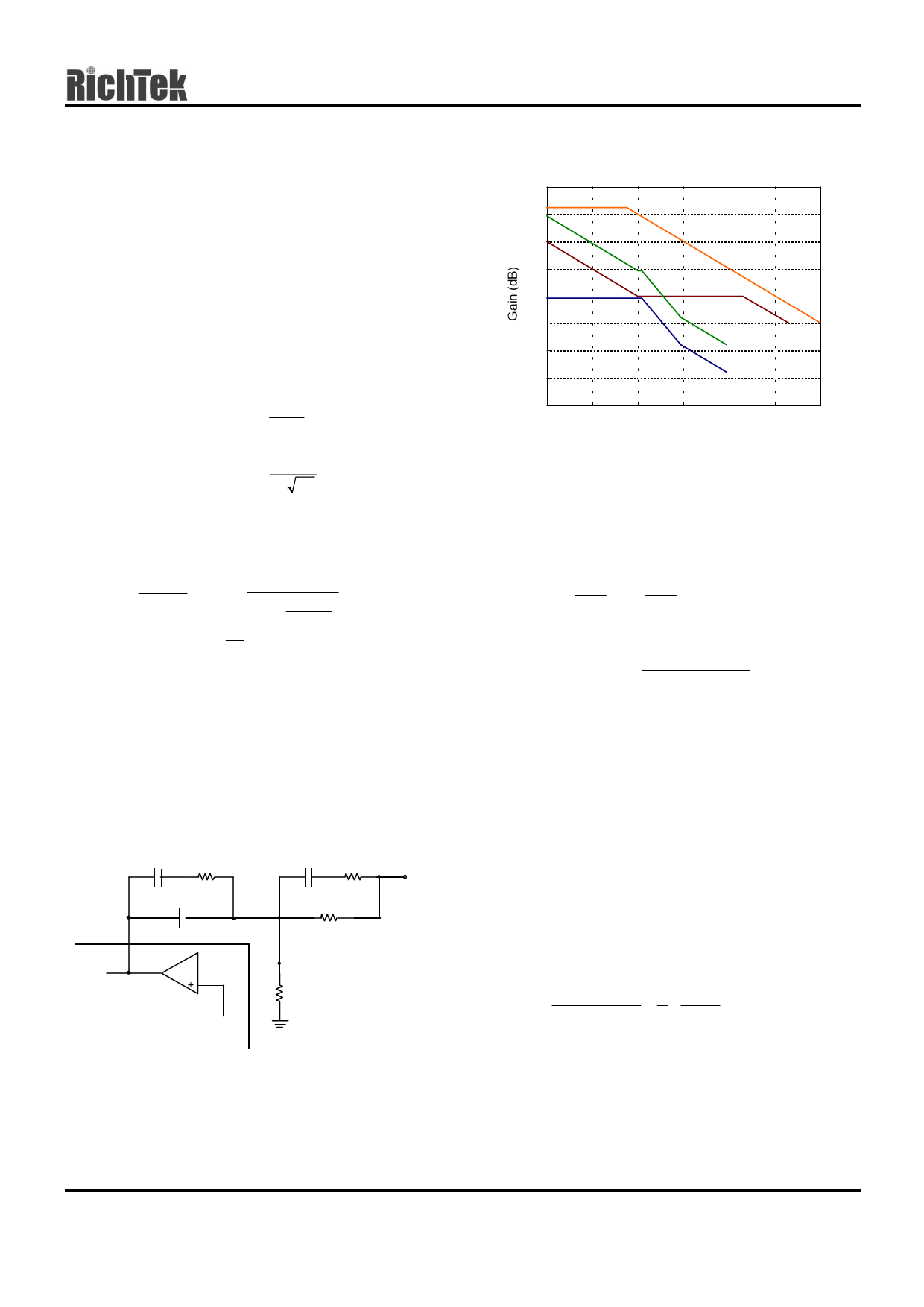
Asymptotic Bode Plot of PWM Loop Gain
100
80
60
Uncompensated EA Gain
40
20
0
Compensated EA Gain
-20
PWM Loop Gain
-40
Modulator Gain
-60
1100
110000
110K00
11000K00 10100000K0 1010M0000 1010000M000
Frequency (Hz)
Fig. 6 Asymptotic Bode Plot of PWM Loop Gain
2. Droop setting
Full load current of each power channel = 60A/3 =
20Amp, the ripple current = ∆IL =
5µS
×
1.5V
2µH
×
1 −
1.5V
12V
=
3.28A
, load current at S/H =
20A −
∆IL
2
= 18.36A , GM
Amp S/H
IX(MAX )
=
RDS(ON) × 18.36A
RSP
,
suggested
IX
at full = 40µA〜50µA, choose RSP = RSN = 2.7KΩ,
IX(MAX) = 40.8µA, required Droop = 120mV =
40.8µA×3×2/3×RADJ ,RADJ = 1.47KΩ.
Take the temperature rising for consideration, if
MOSFET working temperature=70°C and the
temperature coefficient =5000ppm/°C, the
RDS(ON)(70°C) = 6mΩ × {1+(70°C-27°C) ×
5000ppm/°C} = 7.3 mΩ, RADJ(70°C) = RADJ(27°C)
× {RDS(ON)(27°C)/RDS(ON)(70°C)} = 1.21KΩ
3. Over Current Protection setting
OCP trip point current = 30A (at Sample/Hold),
IX
=
RDS(ON) × 30A
RSP
=
3
2
0.6V
× RIMAX
,RIMAX=13.6KΩ
Take the temperature rising for consideration,
RIMAX(70°C) = RIMAX(27°C) ×
{RDS(ON)(27°C)/RDS(ON)(70°C)} = 11.2KΩ
4. SS capacitor
CSS = 0.1µF is the suitable value for most
application.
DS9237-00 January 2002
www.richtek-ic.com.tw
11
Share Link: 