548G-05 Просмотр технического описания (PDF) - Integrated Circuit Systems
Номер в каталоге
Компоненты Описание
Список матч
548G-05 Datasheet PDF : 4 Pages
| |||
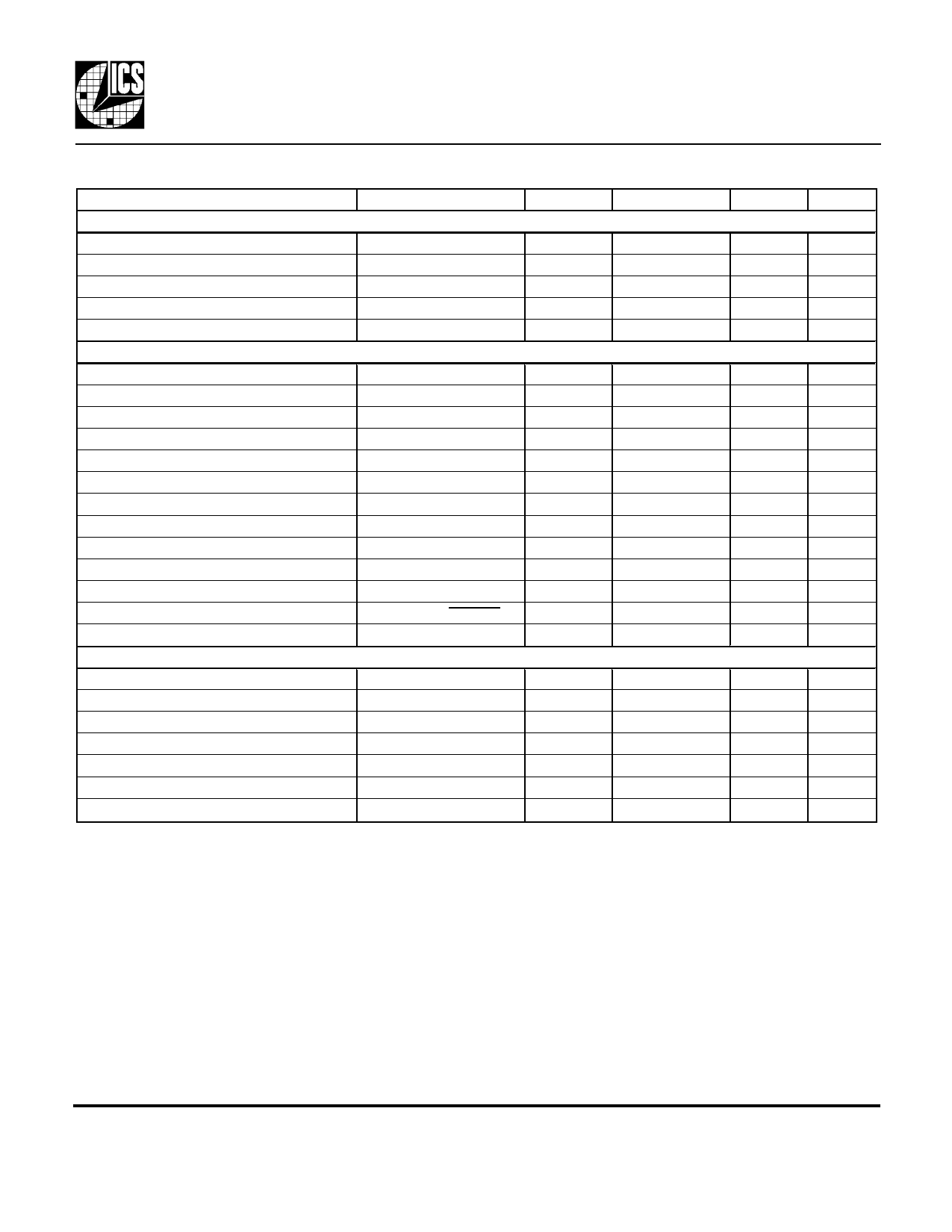
PRELIMINARY INFORMATION
ICS548-05A
MP3 Audio Clock
Electrical Specifications
Parameter
Conditions
ABSOLUTE MAXIMUM RATINGS (note 1)
Minimum
Typical
Maximum Units
Supply voltage, VDD
Referenced to GND
7
V
Inputs and Clock Outputs
Referenced to GND
-0.5
VDD+0.5 V
Ambient Operating Temperature
0
70
°C
Soldering Temperature
Max of 10 seconds
260
°C
Storage temperature
-65
DC CHARACTERISTICS (VDD = 3.3V unless noted)
150
°C
Core Operating Voltage, VDD
2.7
5.5
V
Input High Voltage, VIH, X1/ICLK pin Clock input only
(VDD/2)+1
VDD/2
V
Input Low Voltage, VIL, X1/ICLK pin
Clock input only
VDD/2 (VDD/2)-1 V
Input High Voltage, VIH
2
V
Input Low Voltage, VIL
0.8
V
Output High Voltage, VOH
IOH=-12mA
2.4
V
Output Low Voltage, VOL
IOL=12mA
0.4
V
Output High Voltage, VOH, CMOS level IOH=-4mA
VDD-0.4
V
Operating Supply Current, IDD
No Load
4
mA
Power Down Supply Current, IDDPD
No Load
5
µA
Short Circuit Current
CLK output
±50
mA
Input Capacitance
S0, S1, S2, S3, PDCLK
7
pF
Frequency synthesis error
All selections
AC CHARACTERISTICS (VDD = 3.3V unless noted)
0
ppm
Input Crystal or Clock Frequency
3.6864
MHz
Output Clock Rise Time
0.8 to 2.0V
2
ns
Output Clock Fall Time
2.0 to 0.8V
2
ns
Output Clock Duty Cycle
At VDD/2
40
50
60
%
Start-up Time
VDD=3V to CLK stable
10
ms
Maximum Absolute Jitter, short term
±250
ps
One sigma jitter
70
ps
Note: 1. Stresses beyond those listed under Absolute Maximum Ratings could cause permanent damage to the device. Prolonged
exposure to levels above the operating limits but below the Absolute Maximums may affect device reliability.
External Components/ Application Information
The ICS548-05 requires a minimum number of external components for proper operation. A decoupling
capacitor of 0.01µF should be connected between VDD and GND on pins 3 and 5, as close to the
ICS548-05 as possible. Other VDDs can be connected to pin 3. A series termination resistor of 33 Ω may
be used for each clock output. If REFOUT is not used, then REFEN should be connected to ground. The
input crystal must be connected as close to the chip as possible. The input crystal should be fundamental
mode, parallel resonant. For exact accuracy of the output frequencies, the crystal can be tuned with two
identical capacitors to ground, as shown on the block diagram. The value of these two crystal caps should be
equal to (CL-6)*2, where CL is the crystal load (or correlation) capacitance.
MDS 548-05 AC
3
Revision 032900
Integrated Circuit Systems, Inc. • 525 Race Street • San Jose •CA•95126•(408) 295-9800tel • www.icst.com
Share Link: 