A8740 Просмотр технического описания (PDF) - Allegro MicroSystems
Номер в каталоге
Компоненты Описание
Список матч
A8740
Allegro MicroSystems

A8740 Datasheet PDF : 18 Pages
| |||
A8740
Ultra Small Mobile Phone Xenon Photoflash
Capacitor Charger with IGBT Driver
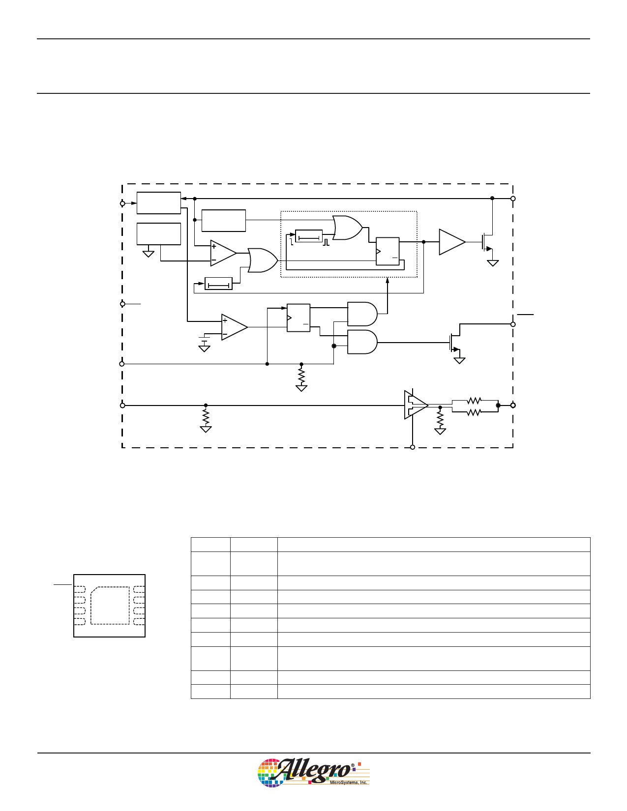
Functional Block Diagram
VBAT
VSW – VBAT
ILIM
Reference
VDSref
VIN_DRV
DCM
Detector
OCP
ton(max)
18 μs
CHARGE
TRIG
toff(max)
18 μs
HmL
Triggered Timer
SQ
RQ
Control Logic
SQ
RQ
Enable
SW
DMOS
DONE
VIN_DRV
IGBT Driver
GATE
GND
Pin-out Diagram
DONE 1
TRIG 2
GATE 3
GND 4
8 CHARGE
7 VIN_DRV
PAD
6 VBAT
5 SW
(Top View)
Terminal List
Number Name
1
¯D¯ ¯O¯ ¯N¯ ¯E¯
2
TRIG
3
GATE
4
GND
5
SW
6
VBAT
7
VIN_DRV
8
CHARGE
–
PAD
Function
Open collector output, pulls low when output reaches target value and CHARGE is
high. Goes high during charging or whenever CHARGE is low.
IGBT trigger input.
IGBT gate drive output.
Ground connection.
Drain connection of internal DMOS switch. Connect to transformer primary winding.
Battery voltage.
Input voltage. Connect to 3 to 5.5 V bias supply. Decouple VIN voltage with 0.1 μF
ceramic capacitor placed close to this pin.
Charge enable pin. Set this pin low to shut down the chip.
Exposed pad for enhanced thermal dissipation. Connect to ground plane.
Allegro MicroSystems, Inc.
3
115 Northeast Cutoff
Worcester, Massachusetts 01615-0036 U.S.A.
1.508.853.5000; www.allegromicro.com
Share Link: